Transition Metal Luminescence in AlN Crystals
- PDF / 381,823 Bytes
- 6 Pages / 414.72 x 648 pts Page_size
- 91 Downloads / 338 Views
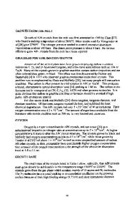
was used. EXPERIMENTAL RESULTS AND DISCUSSION Figure 1 shows a PL spectrum of an AIN needle in the NIR. We observe one weak NP line at 1.043 eV and two intense NP lines peaking at 0.943 eV and 0.797 eV by below bandgap excitation with the 514 nm green line of the Ar ion laser. Only the 0.943 eV luminescence center could be detected under UV excitation, the other two emissions could not be detected by the UV light (360 nm) of the Ar laser. AIN: bulk Ar laser: 514 nm T=2K
"U" C -O
0.943eV
t..o
,_•
1.043eV
0.797eV x4
C t.-'
0~ I .
.
0.7
.
I
0.8
,
,
I
0.9 Energy (eV)
,
,
i
I
,
'
'
1.0
FIG. 1 NIR PL spectrum of an AIN crystalline needle excited with below bandgap excitation of the 514 nm green line of an Ar ion laser. Besides a weak NP line at 1.043 eV we observe two strong emissions peaking at 0.943 eV and 0.797 eV. The 1.043 eV emission Figure 2 (a) shows a more detailed spectrum of the weak 1.043 eV emission. The linewidth is about 2 meV. The defect center shows coupling to phonon modes close to modes observed for AIN in Raman spectroscopy [8]. The peaks in the phonon sideband at 86.3 meV, and 112.8 meV (E1 (LO)) coincide with the modes observed in Raman spectroscopy on the AIN needles. The mode at 77.9 meV is a little lower in energy than the corresponding Raman mode. Thus, this mode is caused by a local mode of the defect. A part of the peak, which is attributed to the phonon at 112.8 meV, belongs to a shoulder of the 0.943 eV emission (see next section). The 1.043 eV luminescence is still visible with about the same intensity at 80 K. We only observe a small shift of about 0.2 meV to lower energy, which is typical for internal electronic transitions of 3d elements [9]. As already pointed out in the introduction internal electronic transitions of the same transition metal ion in GaN and AIN seem to have nearly equal energies. On the basis of this argument the 1.043 eV emission in AIN is caused by the luminescence center responsible for the 1.047 eV emission in GaN[10, 11], which is depicted in the upper spectrum of Fig. 2. This emission is attributed to the 4T 2 -+ 4A 2 transition of a 3d element with a 3d7 electronic configuration. Co 2+ and Ni 3+ are discussed as luminescence centers [10, 11].
614
S(b
"ar C
Ar-Laser: 514 n
*•.93
._1
2A m
77.9 rn*V
r- j.
-26.5
0.95
1.00
meV
1.05
Energy(eV)
Fig. 2. (a) PL spectrum of the 1.043 eV emission in AIN together with the corresponding phonon sideband. The energy values belong to phonon energies and localized vibrational modes. (b) A comparison spectrum of the 1.047 eV luminescence in GaN together with the GaN related phonon sideband. The 0.943 eV emission The emission at 0.943 eV is close to an emission at 0.931 eV in GaN reported by Baur et al. [4]. They observed in temperature dependent PL spectra a hot line 1.6 meV higher in energy. This was their basis to attribute the 0.931 eV emission to an internal electronic transition of V1+. Figure 3 shows the 0.943 eV emission for three different samples. The inset compares two spectra
Data Loading...