Transparent Back Contacts in CdTe/CdS: Evaluation for Tandem Cells
- PDF / 166,828 Bytes
- 6 Pages / 612 x 792 pts (letter) Page_size
- 58 Downloads / 305 Views
1012-Y02-08
Transparent Back Contacts in CdTe/CdS: Evaluation for Tandem Cells Viral Parikh, Anthony Vasko, Alvin D. Compaan, and Sylvain Marsillac Physics and Astronomy, The University of Toledo, 2801 W Bancroft, Mail Stop 111, Toledo, OH, 43606 ABSTRACT CdS/CdTe solar cells with 2.3 µm CdTe were prepared with four different types of p+/n+ transparent back contacts (TBCs) ñ ZnTe:Cu/ZnO:Al, ZnTe:N/ZnO:Al, ZnTe:Cu/ITO, and ZnTe:N/ITO. ZnTe:N/ITO was found to give the best results. This back contact was then used to make cells of lesser (1.8 µm and 0.7 µm) CdTe thickness, in those cases giving good performance up to 9.1% efficiency. Bifacial J-V was performed on all cells with the optimum ZnTe:N/ITO back contact.
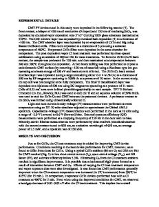
INTRODUCTION CdTe is a promising material for use in solar cells, with single-cell demonstrated efficiencies up to 16.5% [1]. Although the single-junction CdS/CdTe cell should permit significantly higher efficiencies, Noufi, et al [2] have predicted that, with modest improvement in parameters, a tandem device with II-VI alloys having realistic materials parameters could yield conversion efficiencies of 25%. Double-junction devices can be stacked either mechanically (with three or four terminals) or monolithically (with two terminals). Either configuration requires the top cell to have, not only a transparent front contact as usual, but also a transparent and conducting back contact to allow light into the bottom cell. Transparent back contacts also allow characterization from both the ìsunnyî (also called front) and contact (back) side [3], in terms of J-V and quantum efficiency, and we present results on the former here. In the case of monolithically integrated cells, the layers beneath the p-type top cell ideally should be a p+/n+ recombination junction. Such a structure can also function as the back contact for a single top cell. In our experiments, we have used ZnTe:N and ZnTe:Cu as p-type materials, and ZnO:Al and In2O3:Sn (ITO) as n-type materials. We first evaluated the four possible combinations (of two p-type and two n-type) of materials as back contacts for solar cells with 2.3 µm of CdTe, which has been our standard thickness for CdTe cells with metal back contacts. After determining the optimal back contact for our standard thickness, we then prepared cells with that contact with lesser thicknesses. We characterized cell performance with currentvoltage measurements, using either front or back side illumination. Figure 1 shows the cell structure and the direction light enters the structure in the case of front or back side illumination.
Figure 1. Cell structure and meaning of front and back side illumination
EXPERIMENT All cells were prepared on commercially available Pilkington TEC 7 brand fluorinedoped tin-oxide-coated soda-lime glass. All subsequent layers were deposited with rf sputtering and, excepting the reactively sputtered ZnTe:N, in pure argon atmospheres. CdS and CdTe were deposited at 250∞C and 18 mTorr argon pressure. CdS and CdTe were deposited with 35 and 20 watts rf power, resp
Data Loading...