Urbach Edge, Disorder, and Absorption On-set in a-Si:H
- PDF / 124,041 Bytes
- 13 Pages / 612 x 792 pts (letter) Page_size
- 55 Downloads / 311 Views
A1.3.1
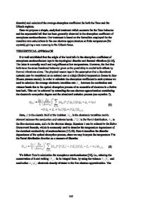
Urbach Edge, Disorder, and Absorption On-set in a-Si:H G. D. Cody Mechanical and Aerospace Engineering, Rutgers University Mail Address: 30 Bainbridge St., Princeton NJ 09540, E-mail: [email protected] ABSTRACT This paper presents a brief review of the research that began in the early '80s, continued through the '90s, and produced a "standard model" for the optical absorption edge of amorphous silicon. The research began as a response to the invention of a-Si:H solar cells by Carlson and Wronski at RCA laboratories in 1976, and the subsequent worldwide interest in the optical characterization of a-Si:H thin films. The immediate need was soon met, but the research continued as an effort to understand the physics of the optical absorption edge in a-Si:H, as well as to understand the differences between, and similarities to, the indirect optical absorption edge of c-Si. In this paper, we highlight the successes of this standard model, and briefly cover its experimental and theoretical development over the last 25 years. We summarize its current status, and suggest some experimental and theoretical opportunities for, and challenges to, what may now be called a standard model for the optical absorption edge of both a-Si:H and a-Ge:H. INTRODUCTION Today the optical properties of amorphous silicon are better known, and understood, than any other amorphous semiconductor, but this was not the case at the time of the 1976 paper of Wronski and Carlson(1), that demonstrated that the glow-discharge decomposition of SiH4 could produce semiconducting thin films of a-Si:H on a variety of substrates, with no inhomogeneities, and densities as high as 96% of crystalline silicon. This discovery occurred at a time of rising national interest in low cost solar electricity, and many government, industrial, and university laboratories started research programs on amorphous silicon as a potential active semiconductor for a variety of thin film semiconductor systems - from solar cells to thin film transistor drives for liquid crystal displays. Optimization of the optical properties of a-Si:H, starting with the independent band model of Jan Tauc(2, 3), was a critical step toward optimization of the performance of thin film solar cells, and the information derived from the optical properties of a-Si:H, was soon employed in the optimization of the electrical performance of these new thin film semiconductors, which today are the dominant drive of flat panel liquid crystal displays. The early device interest in amorphous silicon gave experimentalists access to thin films of unprecedented uniformity, purity, and homogeneity and the consequent reproducibility and scope, of the early experiments, led to novel fundamental optical models of the absorption edge of amorphous semiconductors(4). These models soon led to the first quantitative comparison of the optical absorption edge of an amorphous semiconductor, a-Si:H,
A1.3.2
and its crystalline counterpart, c-Si. In this paper we review the concept of a "standard model for the absorption ed
Data Loading...


