Wet-Etch Patterning of Lead Zirconate Titanate (PZT) Thick Films for Microelectromechanical Systems (MEMS) Applications
- PDF / 1,580,586 Bytes
- 6 Pages / 612 x 792 pts (letter) Page_size
- 63 Downloads / 404 Views
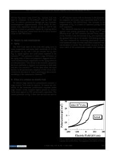
Wet-etch Patterning of Lead Zirconate Titanate (PZT) Thick Films for Microelectromechanical Systems (MEMS) Applications L.-P. Wang, R. Wolf, Q. Zhou, S. Trolier-McKinstry, and R. J. Davis* The Penn State University, University Park, PA16802 * Triquint Semiconductor, 13512 N. Central Expressway, Dallas, TX75243 ABSTRACT Lead zirconate titanate (PZT) films are very attractive for microelectromechanical systems (MEMS) applications because of their high piezoelectric coefficients and good electromechanical coupling. In this work, wet-etch patterning of sol-gel PZT films for MEMS applications, typically with film thicknesses ranging from 2 to 10 microns, was studied. A twostep wet-etch process was developed. In the first step, 10:1 buffered HF is used to remove the majority of the film at room temperature. Then a solution of 2HCl:H2O at 45o C is used to remove metal-fluoride residues remaining from the first step. This enabled successful patterning of PZT films up to 8 microns thick. A high etch rate (0.13µm/min), high selectivity with respect to photoresist, and limited undercutting (2:1 lateral:thickness) were obtained. The processed PZT films have a relative permittivity of 1000, dielectric loss of 1.6%, remanent polarization (Pr) of 24µC/cm2, and coercive field (Ec) of 42.1kV/cm, all similar to those of unpatterned films of the same thickness. INTRODUCTION MEMS, a technology which permits the integration of micromachined mechanical structures with integrated circuits (IC), has been a growing area of research in the last two decades [1,2]. MEMS currently have a wide range of applications including automotive, industrial, biomedical, and information processing [3,4]. Ferroelectric PZT films have been utilized for a variety of applications including microsensors, microactuators, and ferroelectric random access memory [5]. Their high piezoelectric coefficients (d33>100pC/N) and electromechanical coupling (k2~12%) are especially attractive for MEMS sensors and actuators [6]. For these applications, thicker PZT films are usually preferred since the piezoelectric response increases with increasing film thickness [7]. Therefore, patterning techniques for thick PZT films on the micron scale have to be developed. Reactive ion etching (RIE) using capacitive [8], inductive [9], or electron cyclotron resonance (ECR) plasmas [10] has been utilized to pattern PZT films. These studies were driven primarily by ferroelectric memory applications. The film thickness in these applications generally does not exceed 250nm. It has been reported that it is difficult to form volatile species from PZT with etching gases at room temperature; hence, heating the substrate or increasing the ion bombardment energy is generally required for dry-etch patterning. As a result, the etch rate and selectivity with respect to photoresist developed in the above methods are not suitable to etch PZT films for MEMS applications which require 2 to 10 µm thick PZT films. In this paper, a chemical route for patterning thick PZT films is described. EXPERIMENTAL PR
Data Loading...