Wet Etching of Ion-implanted GaN Crystals by AZ-400K Photoresist
- PDF / 783,312 Bytes
- 6 Pages / 612 x 792 pts (letter) Page_size
- 107 Downloads / 312 Views
W11.70
energies were varied between 30 and 180 keV, the ion doses from 1*1014 to 5*1016 ions/cm2. One part of the sample was masked during implantation. Some samples were annealed after ion implantation in a conventional tube furnace up to 1000°C in a N2/10% H2 gas mixture in order to study the damage recovery influence on the etching. The surface morphology of selected samples was investigated by SEM.
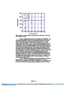
RESULTS A variety of GaN films were used to study the influence of growth method, thickness, carrier concentration and mobility on etching properties. In the first step, the as-grown GaN films were immersed in AZ-400K at room temperature and at 80°C. Some of the GaN films could be etched as grown without any further treatment. Table 1 summarizes the etching results for the different, as grown GaN films. None of the MOCVD GaN films could be etched, whereas 3 out of 4 MBE grown GaN films we studied showed an etching in AZ-400K. We could not observe any influence of film thickness, carrier concentration or mobility on the etching behavior. However, damaging by ion implantation promoted etching. Some of the MOCVD GaN films were implanted with B and Ar ions of different energies and at various ion doses. The first implantation experiments were performed with Ar ions with a constant ion energy of 100 keV and the ion dose was varied between 1015 and 5*1016 ions/cm2. The results are presented in fig. 1. The implanted GaN layers turned brown with increasing ion dose and for the highest ion dose of 5*1016 ions/cm2 a dark brown, metallic shiny layer was obtained. Four-point probe resistivity measurements on a semi-insulating GaN film implanted with 5*1016 Ar ions/cm2 showed a conductance of about 100 (Ωcm)-1.
Table 1: Different types of GaN samples used for etching experiments in AZ-400K, and their etching behavior. Growth type
MOCVD MOCVD HVPE MOCVD MOCVD MBE MBE MBE MBE
Carrier concentration [1/cm3] *1017 1.5 2.5 0.7 3 S.I. 20 0.1 1 10
Thickness [µm]
Mobility [cm2/Vs]
1 hour 25°C
1 hour 80°C
2 1.6 16 3.1 3 2 2.8 1 .3
-15 +9 -630 -300
NO NO NO NO NO YES YES NO YES
NO NO NO NO NO YES YES NO YES
F99W11.70
-230
+5
2500 5e16 1e16 5e15 1e15
Etching depth [Å]
2000
1500
1000
500
0 0
20
40
60
80
100
120
140
T im e [ m i n u te s ]
Fig.1: Dependence of etching depth on etching time for the implantation of 100 keV Ar ions at different ion doses. After ion implantation, the GaN films were immersed in AZ-400K 80°C. Fig. 1 shows the etching depth for different Ar ion doses and etching times. We observe a linear etching during the first five minutes for the highest ion dose (5*1016 ions/cm2, circles). The surface roughness of the etched area is comparable to the one of the untreated surface and amounts to ± 100 Å. After 5 minutes the etching profile seems to saturate at about 1400 Å, which roughly corresponds to the damage region induced by ion implantation, which was calculated/estimated by TRIM [10]. After 60 minutes pores start to develop at the etched surface, up to 1500 Å in depth. Simultaneously with th
Data Loading...