Wiring and introduction of single silicon nanocrystals into multi-walled carbon nanotubes
- PDF / 1,278,430 Bytes
- 6 Pages / 612 x 792 pts (letter) Page_size
- 75 Downloads / 253 Views
A4.5.1
Wiring and introduction of single silicon nanocrystals into multi-walled carbon nanotubes Vladimir Švrček1*, Francois Le Normand2, Ovidui Ersen2, Coung Pham-Huu1, Dominique Begin1, Benoit Louis1, Marc-Jaques Ledoux1 1 LMSPC-ECPM, 25, rue Becquerel, F67087 Strasbourg, France 2 IPCMS, UMR 7504 CNRS, 23 rue du Loess, F-67037 Strasbourg, France, ABSTRACT For a long time the application of silicon technology for optoelectronics has been limited by the extremely poor generation of light by bulk silicon. However, the properties of Si were found to depend on its structure at a nanometric scale and bright photoluminescence from silicon nanocrystals (Si-nc) was discovered. In this work, the results obtained for the mechanical connecting of single Si-nc by two independent techniques are presented. First, the room temperature approach of connecting and introducing Si-nc embedded in colloidal suspensions by capillary forces within multi-walled carbon nanotubes (MWCNTs) and second, the direct growth of MWCNTs on single Si-nc coated with iron catalyst are described. INTRODUCTION In principle, since bulk silicon is an indirect bandgap semiconductor, it could not be used for optoelectronic applications [1]. However, it has been demonstrated that efficient photoluminescence (PL) can be observed from silicon in the form of silicon nanocrystals (Si-nc) of sizes less then 10 nm, i.e. quantum dots [1,2]. In this case, quantum confinement together with surface state effects starts to take place resulting in the opening of the bandgap and in a considerable increase of radiative recombination [2]. The most common techniques used for Sinc fabrication are silicon ion implantation into silicon dioxide (SiO2) thin film, annealing of SiO/amorphous silicon layers and chemical vapor deposition [1]. Such Si-nc shows an adjustable emission wavelength, high emission efficiency, good photostability and broad excitation range. Very often, the problem is the difficulty in achieving Si-nc concentrations high enough to obtain efficient luminescence and transport properties within the surrounding SiO2 matrix. We have developed an alternative concept to synthesize Si-nc by an ex-situ method [3]. We have succeeded on the fabrication of Si-nc with quantum confinement size effect (< 10 nm) by two independent techniques, i.e. a ball-milling technique and pulverized porous silicon [3, 4]. Implementation into colloidal spin on glass (SOG) SiO2 based matrices can offer unique possibilities. For example, it is possible to fabricate either thin films and/or self-supporting samples with high Si-nc concentrations layers with controlling of the luminescence properties of the Si-nc by incorporation them into different host matrix i.e. phosphorous doped silicon [5]. Such Si-nc embedded in SOG maintains its superior luminescence and transport properties while self-supporting layers with high concentrations of Si-nc even exhibit optical gain at room temperature [3,6].
A4.5.2
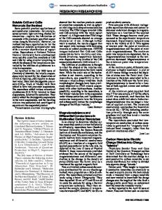
Figure 1. HR-TEM image of silicon nanoparticle dispersed in spin-on-glass with size arou
Data Loading...