X-Ray Diffraction and Reflectivity Studies of Thin Porous Silicon Layers
- PDF / 431,223 Bytes
- 6 Pages / 414.72 x 648 pts Page_size
- 85 Downloads / 234 Views
[8].
437 Mat. Res. Soc. Symp. Proc. Vol. 452 ©1997Materials Research Society
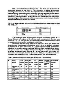
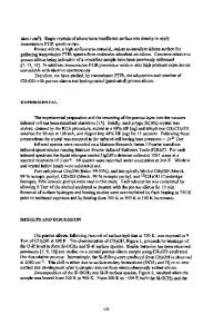
EXPERIMENTAL CONDITIONS We have used (001) Si wafers, positively doped, etched in darkness by an electrochemical process in order to produce a porous silicon (PS) layer at the top surface of the wafer. The electrolyte was composed of I-IF:C 2H 5OH:H 20 (1:2:1) and the value of the applied current density leads to different porosity values. In this paper we report some results obtained on p' type samples (with resistivity p - 0.01 Qcm), of 36% porosity (p'(36%)) and 60% porosity (p'(60%)), and on p type samples (p • 4-6 Qcm) of 65% porosity (p (65%)). The thickness layers (which depends linearly on the anodisation time) were in the 10 nm - 1000 nm range. The X-ray intensity diffracted by the substrate and the porous layer, were obtained with the CuKa radiation of a Philips MRD apparatus [4]. We used the symmetrical diffraction of the (004) reflection in order to be sensitive to the perpendicular lattice misfit. The porous silicon layers have still the properties of nearly perfect single crystal, giving rise to coherent crystal truncation rods through all reciprocal lattice point. Specular X-ray reflectivity investigates the truncation rod through the origin of the reciprocal space. This method allows to investigate the depth profile of the mean electron density. Both methods can be performed by the same experimental geometry using 0o/20 scans which correspond to a displacement along the normal of the sample surface. RESULTS AND DISCUSSION Diffraction measurements The four reflection monochromator and the two reflection analyzer of the MRD apparatus allow a high resolution analysis of the sample structure in the reciprocal space. The introduction of an analyzer allows to separate the coherent diffracted intensity along the crystal truncation rods from the diffuse scattered intensity due to the pore structure. The (o/20 scans obtained along the (004) truncation rod, for a p' (60%) sample and for a p (65%) sample are reported on Fig. 1. -p' (60%): On the experimental curve (dotted line of Fig. la), one observes the Bragg peak of the substrate (S), and the Bragg peak of the thin porous silicon layer (P). The substrate peak width is meanly given by the resolution function of the multiple crystal arrangement. The width of the layer peak is proportional to the inverse of the layer thickness, which is in our case around 520 nm. The elastic expansion of the layers caused by surface effects [4] leads to a perpendicular misfit with respect to the substrate (Aa/a = 8.2 x10⁻⁴) which produces the angular shift of the layer Bragg-peak from the substrate peak. Additionally to the Bragg peaks, one observes several thickness oscillations. From their period one obtains the layer thickness. The high number of oscillations gives evidence for the lateral homogeneity of the sample and the layer thickness. A previous study [7] showed a similar result for low porosity p' samples. To fit the experimental curves one used the dynamical theory of X-ray diffraction,
Data Loading...