ZnGeP 2 and its Relation to Other Defect Semiconductors
- PDF / 3,798,063 Bytes
- 11 Pages / 414.72 x 648 pts Page_size
- 46 Downloads / 336 Views
A.W. VERE, L.L. TAYLOR, P.C. SMITH, C.J.FLYNN, M.K.SAKER, AND J.JONES Defence Evaluation and Research Agency (DERA), St Andrews Road, Malvern, Worcestershire, WR14 3PS, UK [email protected]
ABSTRACT The paper discusses progress in the development of ZnGeP 2 (ZGP) for optical parametric oscillator (OPO) applications and draws parallels with other semiconductors with volatile components, in which the presence of lattice defects gives rise to non-stoichiometry. In particular, attention is drawn to the microprecipitation which accompanies deviation from stoichiometry. In other materials this has been shown to result in spatial non-uniformity in the density of point defects.
INTRODUCTION
A"-B'v-Cv 2 compounds, especially ZnGeP 2 and CdGeAs 2, have been studied for over twenty years [1-6]. Until recently however, synthesis of the compounds and single-crystal growth have been difficult. Problems have included high phosphorus or arsenic pressure at the melting point (1 0270 C for ZnGeP 2; 660'C for CdGeAs 2), mosaic cracking during cooling from the melting point and the presence of optical absorption centres in the OPO pump band. Optical absorption is now the major choke-point in the development of these materials for practical applications such as OPOs and second-harmonic generators. Although substantial improvement has been obtained in the last few years [7][8], the detailed nature of the absorption mechanism remains unclear. There is general agreement that native defects play a controlling role, but vacancy species such as Vz, [9] and the antisite defect ZnIe [10] have both been suggested as the dominant centre. In other semiconductor materials such as GaAs, ZnSe, CdTe and CdHgTe, early research based on photoluminesecence, ESR and ENDOR, also showed the presence of high concentrations of native defects. Subsequent studies however, revealed the controlling influence of relatively low concentrations of residual deep-level impurities [11][l12]. Moreover, the spatial distribution and concentration of other native and impurity defects within the crystal was found to vary according to the dislocation and elastic strain distributions in the ingot and the thermal history of the material [13 -16]. In this paper we report progress in the single-crystal growth of ZGP and review the possible nature of the optical absorption and scattering centres in the light of our observations on other semiconductor materials.
495 Mat. Res. Soc. Symp. Proc. Vol. 484 ©1998 Materials Research Society
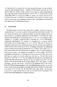
CRYSTAL GROWTH Synthesis of ZGP Early attempts to synthesise ZGP by heating the constituent elements to the melting point inevitably failed, due to premature reaction of zinc and phosphorus to form zinc phosphides, ZGP 18
1200-
1110
1000 Growth furnace
S800600-
E 400Phosphorus furnace 200-
I
I
0
60 120) Time [hrsl Fig.1. Thermal cycle used in the synthesis of MCP Wafertechnology polycrystalline ZGP by horizontalvapour transport
which formed a solid skin over part of the melt, entrapping free phosphorus and resulting in catastrophic ex
Data Loading...