ZnO nanostructures epitaxially grown on ZnO seeded Si (100) substrates by chemical vapor deposition
- PDF / 543,166 Bytes
- 5 Pages / 612 x 792 pts (letter) Page_size
- 86 Downloads / 489 Views
1178-AA06-21
ZnO nanostructures epitaxially grown on ZnO seeded Si (100) substrates by chemical vapor deposition Zhuo Chen1, T. Salagaj2, C. Jensen2, K. Strobl2, Mim Nakarmi1, and Kai Shum1, a 1
Physics Department, Brooklyn College of the City University of New York, 2900 Bedford Avenue, Brooklyn, NY 11210 2
First Nano, a division of CVD Equipment Cooperation, 1860 Smithtown Ave Ronkonkoma, NY 11779 a
[email protected]
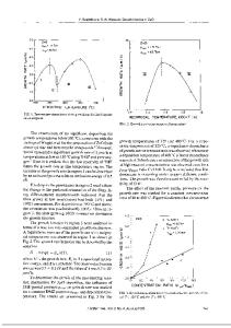
ABSTRACT ZnO nanostructures such as nanowire-networks and vertical nanorods were epitaxially grown on pre-seeded Si (100) substrates by chemical vapor deposition (CVD) method with a solid source. Crystalline ZnO seeds were prepared and controlled by the rapid thermal annealing (RTA) treatment of e-beam deposited amorphous ZnO thin films. Both epitaxially grown ZnO nanostructures and pre-deposited ZnO seeds were characterized by scanning electron microscopy (SEM), and photoluminescence (PL) spectroscopy. Excellent optical characteristics of these nanostructures such as PL line width, linearity of PL intensity as a function of excitation power density were obtained. INTRODUCTION Semiconductor industry continuously brings new inventions into our daily life. For example, the mass-producible and high-quality blue-ultraviolet GaN-based light emitting diodes and lasers are used in blue-ray DVDs, displays, and traffic signals. ZnO is an II–VI semiconductor with a wurtzite structure. It has a wide direct band gap of 3.37 eV [1] at room temperature and a large exciton binding energy of 60 meV [2], theoretically ensuring a more efficient excitonic emission at room temperature than that from GaN counterpart even under low excitation intensity. In attempts to grow high quality ZnO films on suitable substrates using various methods such as metal-organic vapor-phase epitaxy (MOVPE), various ZnO nanostructures, instead, have been successfully grown and characterized. [3-5] In this paper, preliminary experimental data are reported on epitaxial growth ZnO nanostructures on pre-seeded ZnO films by chemical vapor deposition method using a solid source. These ZnO nanostructures are then characterized by scanning electron microscopy and photoluminescence. EXPERIMENTAL DETAILS Because of the large lattice mismatching between crystal ZnO and Si (100), it is difficult to deposit high quality ZnO nanostructure directly on Si (100). A three-step method was investigated in this work. First step, amorphous ZnO films with thickness from 100 to 600 nm was deposited on Si by e-beam evaporator. For the second step, these films were rapidly thermal annealed at 900 oC in Ar gas for 30 minutes. In the last step, a CVD system (First Nano, ET2000) was used for epitaxial growth. This system was
equipped with, a solid source heater, a three-zone (load, center, and end zone) furnace, a quartz paddle/plate/baffle, a gas injector, a vacuum pump and a water cooling system. The ZnO solid source was heated up to 950 oC by a solid source heater. The temperature of reaction zone was controlled by a three-zone furnace to obtain a unifor
Data Loading...