{224} Plane X-Ray Diffraction Study of GaAs on Si Wafers Using a Conventional Double Crystal Diffractometer
- PDF / 327,082 Bytes
- 6 Pages / 420.48 x 639 pts Page_size
- 45 Downloads / 248 Views
{224} PLANE X-RAY DIFFRACTION STUDY OF GaAs on Si WAFERS USING A CONVENTIONAL DOUBLE CRYSTAL DIFFRACTOMETER *J.W.
Lee,
**D.K.
Bowen and *J.P. Salerno
Kopin Corporation, GaAs R&D Laboratory, 695 Myles Standish Blvd., Taunton, MA 02780 **Department of Materials Science and Engineering, MIT, Cambridge, MA 02139 *
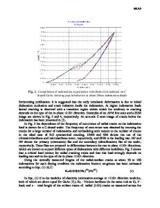
ABSTRACT In an effort to evaluate the near surface crystal quality of GaAs on Si wafers, (2241 plane diffraction were investigated using a conventional double crystal x-ray diffractometer without any high intensity radiation source. The x-ray incident angle to wafer surface varied from 3.6 to 9.6 degrees for different {224) planes due to the substrate tilt angle of 3 degrees. The GaAs to Si rocking curve as the incident angle increased significantly intensity ratio decreased. For the diffraction with 3.6 degree incident angle, only the GaAs peak was detected from the 3.5 um thick GaAs on Si wafer and the GaAs peak became narrower. These indicates that this conventional x-ray diffraction technique is applicable for the near surface quality evaluation of GaAs on Si wafers. INTRODUCTION Material qualities of GaAs epilayers grown on silicon substrates have been improved significantly for the last couple of years. The improvements have been verified by various material characterization techniques as well as various types of device demonstrations. Among them, transmission electron microscopy (TEM) has proved itself the most powerful technique to characterize this heteroepitaxial layer structure. It has taken a key role specifically in nourishing the understanding on the nucleation processes and defect structures[l-3]. However, TEM technique has limitations in sampling time, observation area and strain sensitivity and, in addition, it is destructive. These are significant disadvantages in material development processes. In particular, for the large size diameter wafer process[4,5], which is one of the pronounced potential advantages for this new material system, a comprehensive and nondestructive characterization technique is preferred. The double crystal x-ray diffraction method may be the most appropriate alternative technique suitable for this purpose since it can measure relatively large area wafers in a nondestructive way, and has much greater strain sensitivity. However, a disadvantage of this technique is the penetration depth of the x-ray beam into the GaAs crystal, which is relatively large compared with the usual thickness of an epitaxial GaAs layer. Low incident angle diffraction has been used to ease this problem. In this technique[6] the x-ray incident angle is small and only the diffraction from the near surface crystal planes can be detected. The incident beam is attenuated by extinction and absorption so that the diffracted beam arising from deeper parts of the crystal is very weak or undetectable. To enhance the diffraction signal intensity a high intensity x-ray radiation source is preferred such as the synchrotron radiation or rotating anode. However, these are not commonly available. It is d
Data Loading...