2D Image Sensing Arrays with NIP Diodes
- PDF / 1,746,265 Bytes
- 6 Pages / 414.72 x 648 pts Page_size
- 99 Downloads / 348 Views
2D IMAGE SENSING ARRAYS WITH NIP DIODES C VAN BERKEL, N C BIRD, C J CURLING AND I D FRENCH Philips Research Laboratories, Redhill, Surrey RHI 5HA, UK
ABSTRACT
2D image sensor arrays made with a-Si devices on glass over large area are of considerableinterest as document scanners and in medical applications. We have made a test array containing a-Si NIP diodes for both the sensors and the active matrix switching devices. The issues of vertical crosstalk and image lag are discussed in relationto the device performance of the switching diode. The vertical crosstalk is controlled by the diode capacitance and the image lag by the high transient current in the device. We speculate that the transient current is a trap filling current in the deep states of the switching diode. INTRODUCTION Large area a-Si image sensors have many applications in which the imaged object and image sensor are of similar size, such as document scanning with microlens arrays or in intimate contact mode, or shadow imaging in medical radiography. The sensors consist of either 1D or 2D arrays of a-Si PIN or NIP sensor diodes which integrate the photocurrent to a photocharge, which is then transferred to the external electronics, either directly or via a multiplexing matrix of a-Si switching devices. Either TFTs or diodes can be used as switching devices in these active matrices. a-Si TFTs have a high charge transfer rate, low capacitance and low noise and there are a number of reports on implementations, both in linear"2 and 2D3' 4 arrays. The TFTs have to be fabricated in separate process steps to the sensing diodes and this complicates the manufacturing process. For low cost image sensors, switching and sensing devices should be manufactured 5 simultaneously. It is possible to make photosensitive TFTs alongside the switching TFTs . However, the superb sensor properties of a-Si diodes favour an approach in which both the switches and sensors are made of diodes. PIN switching diodes have been used to make linear sensors up to A4 page width6' 7 , as well as a 2D sensor array8 . The disadvantage of switching diodes lies in a less efficient charge transfer rate and a higher capacitance, which leads to crosstalk. To assess these issues we have fabricated 2D image sensor arrays with aSi NIP diodes and report on some of these issues and their relation to VP-a-Si material properties.
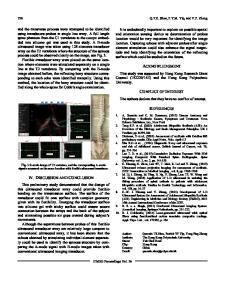
SENSOR TECHNOLOGY Figure 1 illustrates the circuit layout and addressing waveform of the image sensors. Each row of pixels is periodically addressed with a select voltage pulse V,. During the select time t%,
II • ; /:• ... 1
• ts
'Switching Diode Photo Diode Figure 1 Matrix layout and pixel waveform
Mat. Res. Soc. Symp. Proc. Vol. 297. (1993 Materials Research Society
940
F71 AI L-I SiN -
Photodiode
"//
A~/Switch did ode
TO
MCr &Ja-Si =ang
Figure 2 Cross-section of photodiode and switching diode
the total self-capacitance of the photodiode and switching diode is charged up. Then, in the frame time tf, the pixel is discharged by the photocurrent in the photodio
Data Loading...