A Combined TEM/RHEED, SEM/CL Study of Epitaxial GaN
- PDF / 3,079,589 Bytes
- 6 Pages / 414.72 x 648 pts Page_size
- 40 Downloads / 301 Views
Mat. Res. Soc. Symp. Proc. Vol. 482 © 1998 Materials Research Society
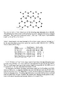
Table 1 Summary of growth conditions used. sample
layer
subst.
substrate preparation
Tsubst
substrate desorbed at
650 C
0
doping
thickness
(or As flux)
(or growth time)
(1.2 x 10⁻⁵ torr of As)
-0.5/4m
GaN
GaP (001) I_ GaP
(As)
(001)
0 620 C.
MG192
GaN
GaAs (001)
substrate desorbed at 0 620 C
700 C
~102°cm-3 Si-doped
MG252
AIN(As) (180A GaAs cap) GaN (As)
GaP (001)
substrate desorbed at 0 620 C
650'C
(1.2 x 10⁻⁵ torr of As)
GaAs (001)
substrate desorbed at 0 620 C; 15min GaAs buffer.
7000C
GaN
GaAs (001)
substrate desorbed at 620°C; 15min GaAs buffer.
700 C
2xl017cm-3 Be-doped 5 (1.2 x 10torr of As) 18 3 2xl0 cmBe-doped (1.2 x 10⁻⁵ torr of As)
GaN
MG79
(As)
MG88
MG260
MG277
(As)
MG338
GaN
MG526
GaN
620°C substrate desorbed at
GaAs {i ii}B
subst. nitrided for 5 minutes as Ts ramped up from 620°C GaAs subst. nitrided for 6 { i ii}B minutes as Ts ramped up from 6000C
6200C 0
0
0
small P3-GaN grains in single crystal GaAs matrix I mixed phase with -O0.5/4m some degree of (1.5 hour) preferred orientation rotated ax-GaN 1.3/4m columnar grains with c-axis in owth direction polycrystalline (2 hours) (1 hour)
(4.2 x 10⁻⁶ torr of As)
700°C
690 C
comment
3
2x10¹⁹cmMg-doped
0.814m
single crystal 3-GaN with anisotropic distribution of
0.8/4m
mix of randomly oriented large grains
0.7pm
cc-GaN with 13-GaN inclusions
2.11m
single crystal (x-GaN
microtwins
lens on opening the camera chamber, and the only waiting time is for the camera chamber to pump down upon changing a specimen. Typically 4 or 5 samples can be examined within an hour. Bulk samples for RHEED observations were routinely plasma cleaned prior to immediate insertion into the microscope. The oxygen/argon plasma was operated at a pressure such that only hydrocarbon deposits were removed from a sample rather than inducing a gentle sputtering action. The effect of this was to minimise background amorphous glow, arising from sample handling, which sometimes hindered RHEED pattern acquisition. Electron transparent foils were prepared in plan view and cross-sectional geometries using conventional techniques [e.g. 6]. The cathodoluminescence (CL) from such foils was examined using an SEM equipped with an Oxford Instruments MonoCL2 system, while complimentary information gained from conventional TEM clarified the nature of the sample fine scale defect microstructure. RESULTS SEM/CL Combined With Conventional TEM The spatial and spectral uniformity of luminescence of TEM GaN foils was characterised using SEM/CL. The spectrum shown in Fig. la was recorded from a plan view nominally single crystal wurtzite GaN foil cooled to liquid nitrogen temperature. The two peaks in the CL spectra at 357.8nm and 386nm were used to form the images of Figs. lb and Ic. These peaks are centred at 3.47eV and 3.21eV corresponding to the ox and 0 phases of GaN respectively. The complimentary conventional TEM image from this plan view sample (Fig. ld) reveals t