A Comparative Study of MOCVD Produced ZnO Films Doped with N, As, P and Sb
- PDF / 194,697 Bytes
- 5 Pages / 612 x 792 pts (letter) Page_size
- 99 Downloads / 263 Views
0957-K07-48
A Comparative Study of MOCVD Produced ZnO Films Doped with N, As, P and Sb Gary S. Tompa, S. Sun, C. E. Rice, L. G. Provost, and D. Mentel Structured Materials Industries, Inc., 201 Circle Drive N., Unit 102/103, Piscataway, NJ, 08854
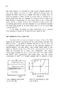
ABSTRACT ZnO thin films are of interest for an array of applications; including: light emitters, photovoltaics, sensors and transparent contacts among others. Of particular interest is the potential to produce p-type layers from which p-n junction devices could be routinely produced. While it is fairly routine for MOCVD to produce n-type films with doping concentrations in the 10E20 cm-3 range and resistivities below 10E-3 ohm-cm; it is very difficult to produce measurable p-type ZnO. We report on our efforts with doping films p-type using N gas sources and metalorganic sources of P, As, and Sb. Films showing acceptor bands by photoluminescence have been demonstrated; however reliable electrical measurements remain difficult. Specific problems include achieving low resistance ohmic contacts, accounting for the photoresponsiveness of ZnO films and sensitivity limits in Hall measurements of low-doped and compensated materials. The presentation will review deposition parameters, produced and processed films and material characteristics. INTRODUCTION ZnO, a wide-bandgap (3.437 eV at 2 K) semiconductor material, is presently receiving wide attention because of fundamental advantages over GaN in the quest for blue/UV light emitters and detectors, and high-speed, high-power, high-temperature electronic devices1. For example, ZnO has a higher exciton binding energy than that of GaN, a higher theoretical saturation velocity, and a higher radiation tolerance. The principal roadblock to achieving these devices has been the difficulty in preparing p-type ZnO repeatably and reliably. Interest and research on the deposition of p-type ZnO has exploded recently. The first Ndoped p-type film was reported in 1997.2 Since then a large number of groups have also achieved p-type conductivity in thin film samples, principally using N, P, and As as dopants. A variety of growth techniques have been used in the growth of these films, including sputtering,3 pulsed laser deposition (PLD),4 molecular beam epitaxy,5 MOCVD,6 and others. At SMI, we have developed Low Pressure (and Plasma Enhanced) Metal Organic Chemical Vapor Deposition (LP-MOCVD) systems to produce an array of oxides. The system employs a vertical high speed Rotation Disk Reactor (RDR), with radially distributed multi-gasinjectors on its top flange (for uniformity over large areas) and a separate oxygen injector directly above the sample platter (minimizing pre-reactions). The high speed rotating disk can be rotated through 1000 RPM. The high speed rotation and high gas velocity induces laminar, non-recirculating forced convection flow in the system. Samples are heated by a fixed radiative heater below the rotating susceptor. Thermophoresis drives particles from the deposition surface. The temperature, pressure, rotation, and mass-flo
Data Loading...