A Comparative Study of Nickel Silicide Formation Using a Titanium Cap Layer and a Titanium Interlayer
- PDF / 864,309 Bytes
- 6 Pages / 612 x 792 pts (letter) Page_size
- 1 Downloads / 359 Views
A COMPARATIVE STUDY OF NICKEL SILICIDE FORMATION USING A TITANIUM CAP LAYER AND A TITANIUM INTERLAYER W.L. Tan1, K. L. Pey1, Simon Y.M. Chooi2, J.H. Ye3 Center for Integrated Circuit Failure Analysis and Reliability, Faculty of Engineering, National University of Singapore, 4 Engineering Drive 3, Singapore 117576, Singapore. 2 Department of Technology Development, Chartered Semiconductor Manufacturing, 60 Woodlands Industrial Park D Street 2, Singapore 738406, Singapore. 3 Institute of Materials Research and Engineering, 3 Research Link, Singapore 117602, Singapore.
1
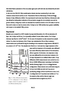
ABSTRACT NiSi formation is known to be hindered by interfacial native oxide. Such oxide is easily formed on the Si surface through inefficient cleaning or a long time lag prior to Ni deposition. In this study, two methodologies were investigated to remove this layer of native oxide when no DHF clean was performed prior to metal deposition. Firstly, the deposition of a 100Å Ti cap layer after Ni deposition and secondly, the deposition of a middle 50Å Ti prior to Ni deposition. The samples were then rapid thermal annealed from 500 to 800°C. It was found for the Ti / Ni / SiO2 / Si stack, a layer of NiSi was formed starting from 600°C. Transformation to the NiSi2 phase begins at 750°C. As for the Ni / Ti / SiO2 / Si stack, a layer of NiSi was formed after 500°C annealing and conversion to NiSi2 also took place at 750°C. However, it was found that at low temperatures such as 500-600°C, facets of NiSi2 were identified under the thick NiSi layers, embedded in the Si substrate. Ternary phases like TixNiySiz were also identified at the surface of the sample.
INTRODUCTION Self aligned silicides (Salicides) are used in the manufacturing of CMOS to reduce sheet resistance and contact resistance at the gate, source and drain areas. Currently, the most common salicide materials are TiSi2 and CoSi2. Although TiSi2 has been widely used in the past few generations, its sheet resistance is found to be line-width dependent for narrow lines of less than 0.35µm [1-3]. CoSi2, on the other hand, do not exhibit any line width dependence, but is subjected to oxide contamination problems and high leakage currents [4,5]. Therefore, NiSi is being introduced as the next generation salicide material. Besides having a low Si consumption [6] which makes it suitable for ultra-shallow applications, its sheet resistance is also line-width independent like CoSi2 [7]. The integration of NiSi in IC fabrication is made simpler as only a single annealing step between 400 to 700°C is required. Studies performed on CoSi2 formation have found that a Ti cap layer protects the underlying films from oxide contamination from the ambient as well as remove the interfacial oxide between Co and Si [8]. In a technique known as Ti interlayer mediated epitaxy (TIME), a thin Ti interlayer is not only able to reduce interfacial oxide contamination, but also control the Co flux, thus forming epitaxial CoSi2 [4,5]. K6.6.1
The formation of NiSi is also found to be sensitive to oxide contaminations. In th
Data Loading...