A Fast Laser Alloying Process for the Selective Electroplating of Metal on SiO 2 and Polyimide
- PDF / 1,085,574 Bytes
- 6 Pages / 420.48 x 639 pts Page_size
- 98 Downloads / 332 Views
A FAST LASER ALLOYING PROCESS FOR THE SELECTIVE ELECTROPLATING OF METAL ON Si02 AND POLYIMIDE
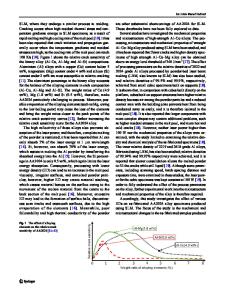
VINCENT MALBA AND ANTHONY F. BERNHARDT, Lawrence Livermore National Laboratory, P.O. Box 808 L-271, Livermore, CA 94550 ABSTRACT A new laser direct-write process for patterning of metal on multichip modules has been developed. The process involves the laser modification of the non-conductive surface of a seed multilayer, converting it to a conductive surface, which can be electroplated with metal. The seed multilayer is composed of a TiW adhesion layer, onto which a Au film is sputtered, followed by an a-Si layer, which forms the non-conductive surface. The laser modifies the surface by alloying (or mixing) the Si and Au to form the conductive surface. This laser process has been shown to be capable of writing speeds of 2.5 m/s. With a silicon dioxide interlevel dielectric layer, the process works over a large range of laser power (Pmax/Pmin - 5). A polyimide interlevel dielectric layer can be used without damage or loss of adhesion, although the process margin is substantially reduced (Pmax/Pmin - 2). INTRODUCTION Multichip modules (MCM) are revolutionizing microelectronics packaging [1-3]. Laser patterned chip-to-board interconnects can be used in place of wire bonds or TAB to reduce electrical parasitics, and the discretionary nature of the laser process compensates for die placement errors [4,5]. A major drawback to commercialization has been the slow speed of laser deposition and etching. Recently, processes have been developed which use laser activation of a conventionally deposited seed layer, followed by metallization with selective CVD [6] or electroless plating [7]. These processes are considerably faster than laser deposition and etching, and represent a class of processes which have the potential of making laser direct-writing viable. Based on the seed layer approach, a process has been developed for metallizing MCM interconnects that is capable of writing speeds as high as 2.5 m/s [8]. An Ar ion laser is used to modify the surface of a multilayer film, changing the insulating surface into a conductor in the areas the laser has scanned. The surface layer is a-Si, which absorbs the laser beam, and mixes with an underlying layer of gold as shown in Figure 1. The surface areas which are conductive can be electroplated; the gold layer serves to conduct the current. Electroplating produces Mat. Res. Soc. Symp. Proc. Vol. 236. ®1992 Materials Research Society
92
high conductivity lines at a rate orders of magnitude faster than electroless plating. The seed layer is then removed from the substrate, leaving a plated line standing on a dielectric layer.
So a-Si
Au
T~wLaser
/
TiW
a. Deposit seed layer
b. Laser pattern
c. Electroplate copper
d. Remove seed layer
Figure 1.
Schematic of the laser alloying process
The laser alloy process was developed for use with a silicon dioxide dielectric layer, but many other MCM technologies rely on polyimide dielectric layers. It is more difficult to laser write on pol
Data Loading...