Effect of SiO 2 Capping Layer on a Laser Crystallization of a-Si Thin Film
- PDF / 1,305,750 Bytes
- 6 Pages / 612 x 792 pts (letter) Page_size
- 1 Downloads / 454 Views
A17.3.1
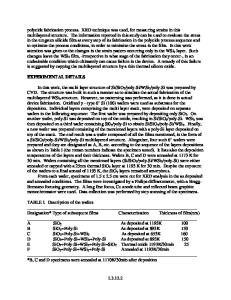
Effect of SiO2 Capping Layer on a Laser Crystallization of a-Si Thin Film Myung-Koo Kang, Hyun Jae Kim, Sook Young Kang, Su-Kyung Lee, Chi-Woo Kim and Kyuha Chung LTPS Group, Flat Panel Display R&D Team, Samsung Electronics Co., Yongin-City, Gyeonggi-Do, Korea 449-711 ABSTRACT Effect of SiO2 capping layer(C/L) on recrystallization of amorphous Si (a-Si) film was investigated. When a thick C/L over 500 Å was deposited on an a-Si film before crystallization, fine p-Si grains less than 100nm were obtained at full range of energy density window. However, when a thin C/L below 200 Å was used, Si-melt spouted out through C/L at over critical energy density. When Si-melt started spouting, abrupt change of grain size also occurred. These large grains could be explained by a non-uniformity of heat flow caused by Si-melt spouting. With this polycrystalline Si (p-Si) material having appreciable grain size protected by C/L, fabrication of low-cost Low Temperature Poly Si (LTPS) without additional cleaning of p-Si surface could be successfully developed. INTRODUCTION Polycrystalline-silicon (p-Si) thin-film transistors (TFTs) are used in a variety of applications, including large-area electronics [1] and vertically stackable components for three-dimensional integration [2]. P-Si is typically fabricated from amorphous Si (a-Si) thin-film deposited on an inexpensive glass, such as Corning 1737, which has a quoted working range below 600°C. Various recrystallization technologies of a-Si film have been developed to meet this temperature limitation of glass. Among various recrystallization technologies, the excimer laser method has been commonly adopted in commercial fields. In this method, a pulsed laser is used for irradiating on an a-Si precursor film. It is absorbed by a film surface and induces instant melting and solidification. The short pulse duration of the laser beam prevents sustained heating of the underlying substrate, and makes the process compatible with glass substrate [3]. The crystallinity is superior to that of other crystallization techniques such as SPC (Solid Phase Crystallization) because the transformation from a-Si to p-Si is occurred via melting and re-solidification process. In the mean time, the property of p-Si TFTs is mainly dependent on grain boundaries within channel and a surface morphology. To minimize the number of grain boundaries within the channel area, new technologies such as SLS [4] (Sequential Lateral Solidification) or MILC
Downloaded from https://www.cambridge.org/core. Access paid by the UCSB Libraries, on 11 Mar 2018 at 10:37:29, subject to the Cambridge Core terms of use, available at https://www.cambridge.org/core/terms. https://doi.org/10.1557/PROC-762-A17.3
A17.3.2
(Metal Induced Lateral Crystallization), which can make large lateral grains, have been developed. Grain boundary passivation technique [5] has been also developed to decrease a boundary trap density. However, it is more difficult to improve the surface structure because a surface morphology after laser crystal
Data Loading...