A Novel Room Temperature Infrared Detector Using Micro-Compensated Amorphous Silicon
- PDF / 879,733 Bytes
- 5 Pages / 414.72 x 648 pts Page_size
- 79 Downloads / 270 Views
ABSTRACT Detection at room temperature of near and medium infrared radiation has been achieved by using micro-doped or micro-compensated amorphous silicon films as intermediate absorber layer in a p-n junction. Extremely low dopant concentrations in the gas mixture have been utilized to achieve micro-doping and micro-compensation. Device operation is based on transitions, induced by the infrared radiation, between extended states in the valence band and defects in the forbidden gap. The absorption process changes electron defect occupancy, giving rise to change in electric field distribution. This effect can be observed as variation of differential capacitance of the structure. Capacitance measurements, performed on two different devices with micro-doped and micro-compensated absorber layer respectively, showed sensitivity to radiation from 900 nm up to 4.5 jim. INTRODUCTION Several attempts to use amorphous silicon (a-Si:H) films detection of near infrared radiation has been done in the past. Photodetection up to 900 nm was obtained by using amorphous silicon-germanium alloys [ 1, 2], taking advantage of the narrow energy band-gap of this material. Detection of longer wavelength was achieved by Okamura and Suzuki [3], who presented an avalanche a-Si:H photodiode with sensitivity in the 1.3 lgm-1.55jtm range, and by Wind and MUller, who reported [4] infrared response of a-Si:H p-i-n diodes up to 2400 nm under forward bias, deposited from undiluted SiH4 by plasma enhanced CVD. In this paper we demonstrate detection at room temperature of near and medium infrared
(IR) radiation by a novel amorphous silicon device, which operation is based on transitions induced by the IR radiation between valence band and localized states. IR radiation
-Ona-Si:H
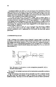
Fig. 1 Structure of amorphous silicon IR detectors. 219 Mat. Res. Soc. Symp. Proc. Vol. 507 ©1998 Materials Research Society
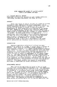
30 ,- 2 5 2
¢.-
... ..o ......................................................................................................C"O IR 3.25-4.31:m
10 ....
10-zi-
101 0 Frequency (kHz)
Fig. 2 Capacitance versus frequency measured on p-c-n device at zero bias voltage, in dark 2 condition and under IR radiation: 3.25-4.3 jim, 500 jtW cm- .
EXPERIMENTAL RESULTS A cross-section view of the detector is shown in Fig. 1 [5]. The device structure is similar to a conventional p-i-n structure, where the separation layer includes very low concentrations either of boron atoms or of phosphorous and boron atoms together. The whole structure was deposited from Sill4 by plasma enhanced CVD. The substrate temperature was 250 0C and the gas pressure was 300 mTorr. We realized two different devices. In the first, the central layer was deposited with 0.25 ppm of PH 3 and 18 ppm of B 2H6 in the gas mixture. We labeled this material c and we refer to the structure as p-c-n device. The second structure was obtained depositing the central layer with 200 ppm of B 2H6 in the gas mixture. We called this material p-, and we refer to the structure as p-1p-n device. In both
Data Loading...