Large Area Position Sensitive Detector Based on Amorphous Silicon Technology
- PDF / 844,705 Bytes
- 6 Pages / 414.72 x 648 pts Page_size
- 91 Downloads / 365 Views
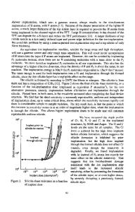
LARGE AREA POSITION SENSITIVE DETECTOR BASED ON AMORPHOUS SILICON TECHNOLOGY E. Fortunato, M. Vieira, L. Ferreira*, C. N. Carvalho, G. Lavareda and R. Martins Dept. Science Materials, Faculty of Science and Technology, New University of Lisbon 2825 Monte de Caparica, Portugal *EID, Optoelectronic Dept., Quinta dos Medronheiros, 2825 Monte de Caparica, Portugal ABSTRACT We have developed a rectangular dual-axis large area Position Sensitive Detector (PSD), with 5 cm x 5 cm detection area, based on PIN hydrogenated amorphous silicon (a-Si:H) technology, produced by Plasma Enhanced Chemical Vapor Deposition (PECVD). The metal contacts are located in the four edges of the detected area, two of them located on the back side of the ITO/PIN/Al structure and the others two located in the front side. The key factors of the detectors resolution and linearity are the thickness uniformity of the different layers, the geometry and the contacts location. Besides that, edge effects on the sensor's corner disturb the linearity of the detector. In this paper we present results concerning the linearity of the detector as well as its optoelectronic characteristics and the role of the i-layer thickness on the final sensor performances. INTRODUCTION Up to now, crystalline silicon have been used to produce PSDs. Nevertheless its detection area is small (around I x 1 cm 2), which implies the need of expensive and complicated optical magnification systems for supporting their field of applications towards large area inspection systems. Amorphous silicon based devices is now well established as a viable low-cost technology for a variety of large area applications, such as solar cells [1], image sensors [2], flat panel displays [3], etc.. These devices take advantages of certain amorphous silicon film properties such as: low temperature processing capability; high photosensitivity; short response time; thermal stability and high production yield. The application of a-Si:H to PSDs have already been used for a digitezer, an image transfer system [4] and for a telephone terminal [5]. In this paper we report results concerning the application of a-Si:H to rectangular dual-axis position sensitive detectors and its correlation with film properties. The obtained results are quite promising making possible the application of these sensors to a wide variety of optical inspection systems such as: machine tool alignment and control; angle measuring; rotation monitoring; surface profiling; medical instrumentation; targeting; remote optical alignment; guidance systems; etc., to which inspection automated control is needed. OPERATING PRINCIPLE The PSD is an optoelectronic sensor that provides continuos position data of a light spot traveling over its surface. Compared to the discrete element detectors such as CCDs (Charge Coupled Devices), the PSD features high position resolution, fast response speed, and simple operating circuits. Thus, when a light spot falls on the PSD, an electric charge proportional to the light energy is generated at the incident
Data Loading...