A novel terbium doping effect on physical properties of lead sulfide nanostructures: A facile synthesis and characteriza
- PDF / 1,216,255 Bytes
- 12 Pages / 584.957 x 782.986 pts Page_size
- 82 Downloads / 283 Views
A novel terbium doping effect on physical properties of lead sulfide nanostructures: A facile synthesis and characterization Mohd. Shkir1,a) , Kamlesh V. Chandekar2, Thamraa Alshahrani3, Ashwani Kumar4, Salem AlFaify1 1 Advanced Functional Materials and Optoelectronics Laboratory (AFMOL), Department of Physics, College of Science, King Khalid University, Abha 61413, Saudi Arabia 2 Department of Physics, Rayat Shikshan Sanstha’s, Karmaveer Bhaurao Patil College, Vashi, Navi Mumbai 400703, India 3 Department of Physics, College of Science, Princess Nourah Bint Abdulrahman University, Riyadh 11671, Saudi Arabia 4 Department of Physics, IK Gujral Punjab Technical University, Kapurthala 144603, India a) Address all correspondence to this author. e-mail: [email protected]
Received: 23 April 2020; accepted: 30 July 2020
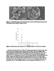
Lead sulfide (PbS) is having tremendous applications in the field of optoelectronics. Hence, a facile low temperature synthesis of PbS with different contents of terbium (Tb) has been achieved and investigated for structure–optic–dielectric–electrical properties. The structure confirmation was observed through the X-ray diffraction and Rietveld refinement process which approved a monophasic cubic structure. Rietveld refinement gives a best-fitting profile of the prepared products. The crystallite size was estimated to be in range of 15–21 nm. FT-Raman study also approved the single-phase PbS with all characteristic modes. For further confirmation of composition, homogeneity, and Tb in the final product, the EDX/SEM e-mapping was carried out. The morphological investigation was carried out through SEM which revealed that the shape and size are greatly influenced by Tb content addition in PbS. The energy gap (Eg) was estimated in the range of 1.42–1.62 eV for all Tb@PbS, and the largest Eg value was observed for 0.5 wt% Tb@PbS. The dielectric constant values are calculated in the range of 16–25 in the tested frequency region. The ac electrical conductivity was enhanced with frequency, and a charge transport mechanism is related to a correlated barrier hoping model in the prepared samples.
Introduction Lead sulfide (PbS) is one of the most important semiconductor material among IV–VI group due to its narrow direct band gap of bulk PbS (0.4 eV, 298 K) [1] and a large excitation Bohr radius (18 nm) [2]. Moreover, its absorption coefficient increases from the infrared to visible region [3], and it shows quantum confinement, which reveals the size-dependence electronics and optical properties of nanoparticles [4]. PbS also shows good photoconductivity activity in a near-infrared region and 3rd-order nonlinear optical property [5, 6] and photocatalyst activity. The intrinsic physical properties of PbS material make it suitable for various applications including a light-emitting diode as electroluminescent and optical switch devices due to unique optical property [7] and infrared sensor (detector) with a broad spectral response up to 4 μm [8, 9]. In addition
© Materials Research Society 2020
to this appl
Data Loading...