A Study of Indium Nitride Films Grown Under Conditions Resulting in Apparent Band-gaps from 0.7 eV to 2.3 eV
- PDF / 256,752 Bytes
- 6 Pages / 612 x 792 pts (letter) Page_size
- 108 Downloads / 290 Views
L11.23.1
A Study of Indium Nitride Films Grown Under Conditions Resulting in Apparent Band-gaps from 0.7 eV to 2.3 eV 1
1
3
3,4
5
K. S. A. Butcher , M. Wintrebert-Fouquet , Motlan2, S. K. Shrestha , H. Timmers , K. E. Prince and T. L. 1 Tansley 1 Physics Department , Macquarie University, Sydney, NSW 2109, Australia. 2 Department of Physics, Faculty of Mathematics and Science, State University of Medan, Indonesia. 3 School of Physics, University of New South Wales at the Australian Defence Force Academy, Canberra, ACT 2600, Australia. 4 Department of Nuclear Physics, Research School of Physical Sciences and Engineering, Australian National University, Canberra, ACT 0200, Australia. 5 Australian Nuclear Science and Technology Organisation, Private Mail Bag 1, Menai NSW 2234, Australia. ABSTRACT The band-gap of indium nitride has long been believed to be about 1.9eV with slight variations due to band-tailing in polycrystalline samples and degenerate doping. Recently, other values as low as 0.7 eV have apparently been observed. We have compared samples spanning this apparent range of band-gap using secondary ion mass spectroscopy (SIMS), X-ray Photoelectron Spectroscopy (XPS) and heavy ion elastic recoil detection analysis (ERDA), in conjunction with spectral optical density measurements. Once structural inhomogeneiteies are taken into account, we show that much of the conflicting data are compatible with direct photoionisation with a threshold energy of about 1.0eV. This feature was first reported in polycrystalline indium nitride over 15 years ago and attributed to a |p> like defect state. We ask whether the feature may instead be a direct band-gap.
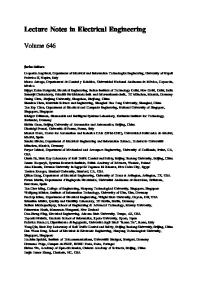
INTRODUCTION Indium nitride is potentially a very high mobility material, but preparation of satisfactory samples has proven difficult and many of its basic properties are still being assessed. A group of low carrier concentration polycrystalline thin films were grown by RF sputtering in the early 1980s, with one having a mobility of 2700 cm2/V⋅s for a carrier concentration of 5x1016 cm-3 [1]. Those samples, along with a series reported by other workers, established an optical transmission band-gap of 1.89 eV in the low-concentration limit [2] with a systematic carrier concentration dependence ascribed to a Moss-Burstein shift. Recent MBE InN has been reported to have other band-gaps, apparently as low as 0.7 eV [3-5]. Oxygen has been suggested as being responsible for the 2 eV band-gap. A counter view is that the lower band-gap 70x10 material may be metal rich as a result of growth near the InN 60x10 300x10 decomposition temperature. Figure 1 illustrates the point by 50x10 200x10 E = 2.7 eV 100x10 showing the well known reduction in the band-gap of GaN 40x10 30x10 2.5 3.0 3.5 grown under metal rich conditions (inset). 20x10 We have carried out a series of measurements in an effort E = 3.35 eV 10x10 0 to gain a better understanding of the spread of observed band1 2 3 4 5 Energy (eV) gap values. Films from three different laboratories were analysed. MBE grown InN fr
Data Loading...