A Study of Point Defects and Cause of Nonstoichiometry in InSb Nanowires
- PDF / 530,739 Bytes
- 6 Pages / 612 x 792 pts (letter) Page_size
- 62 Downloads / 275 Views
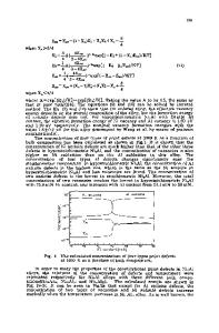
A Study of Point Defects and Cause of Nonstoichiometry in InSb Nanowires U. Philipose, Gopal Sapkota, Pradeep Gali and Prathyusha Nukala Department of Physics, University of North Texas, 1155 Union Circle, TX 76203-5017, U.S.A ABSTRACT Synthesis of InSb nanowires using chemical vapor deposition (CVD) is technically challenging due to the tuning of III-V vapor pressures. Growth parameters such as the choice of the metal catalyst, growth temperature and vapor pressure of constituents affect the morphology and stoichiometry of InSb nanowires. By controlling the growth temperature, it was possible to grow either stoichiometric InSb nanowires or In nanowires that contained no Sb within detectable limits. We present a simple model to show that the occurrence of native point defects in InSb is influenced by the growth kinetics and by the thermodynamics of defect formation. Results from this model are in good agreement with our experimental findings of the evidence of point defects in these nanowires. INTRODUCTION InSb is a promising III–V direct band gap semiconductor, and is used in the fabrication of infrared detectors, including thermal imaging cameras, and infrared astronomy [1, 2]. It has a very narrow band gap of 0.17 eV at 300 K, and hence near band edge absorption occurs in the infrared range. It is hence a promising material for photodetectors, sensitive in the 1–5 μm wavelength range. In addition InSb has several attractive properties like very high electron mobility (7.8 m2 V−1 s−1), and large ballistic length (up to 0.7μm at 300 K). These properties make InSb a promising candidate for several device applications, including high speed fieldeffect transistors, thermoelectric power generation, and cooling devices. In recent years, InSb has attracted attention due to the fact that InSb photo-voltaic detectors can cover a spectral response range equivalent to PbSe and PbS photo-conductive detectors, but with higher response speed and better signal-to-noise ratio [3-5]. Synthesis of crystalline InSb as a low dimensional system coupled with its many advantages could lead to the realization and development of an entirely new branch of nanoscale optoelectronic devices. The challenge in growing InSb nanowires is in maintaining the stoichiometry of the growing crystal. The growth window for synthesis of stoichiometric InSb nanowires by conventional CVD techniques is very narrow, due to the significant partial pressure difference between In and Sb vapors in contact with the InSb crystal [6, 7]. The purpose of this paper is to investigate the stoichiometry of the InSb nanowires as a function of growth parameters and to explain deviations from stoichiometry by determining the concentration of intrinsic point defects in the nanowire. We find that outside the narrow growth temperature window, it was possible to grow nanowires that are In rich or Sb rich. EXPERIMENT InSb nanowires were grown on Si substrates using vapor assisted VLS growth [7]. Two types of seed layers (metal catalysts) were used in the growth of these nanowire
Data Loading...


