Single Crystal InSb Nanowires: Synthesis, Characterization, Properties and Applications
- PDF / 5,254,604 Bytes
- 6 Pages / 612 x 792 pts (letter) Page_size
- 35 Downloads / 361 Views
0940-P07-05
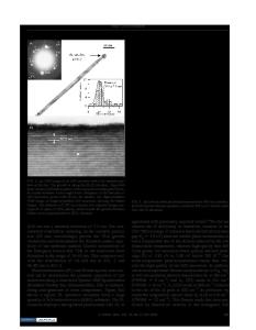
Single Crystal InSb Nanowires: Synthesis, Characterization, Properties and Applications Qi Laura Ye1,2, Toshishige Yamada1, Hongbing Liu2, Raymond Scheffler1,2, Natalio Mingo1, and Ryan Leverenz1,2 1 Center for Nanotechnology, NASA Ames Research Center, Mail Stop 229-1, Moffett Field, Mountain View, CA, 94035 2 ELORET, 465 S. Mathilda Ave., Suite 103, Sunnyvale, CA, 94086 ABSTRACT We report the first large-scale synthesis of single crystal InSb nanowires using selfcatalyzed vapor-liquid-solid (VLS) transport process. Narrow growth window for achieving single crystal InSb nanowires has been discovered. Our batch fabricated InSb nanowires are 50180 nm in diameter and 10-30 µm in length. Materials composition analysis by EnergyDispersive X-ray Spectroscopy (EDAX) reveals that the as-grown InSb nanowires are pure single crystals of InSb. Structural analysis by High Resolution Transmission Electron Microscopy (HRTEM) and Selected Area Electron Diffraction (SAED) reveals that InSb nanowires have cubic crystal structures. The nanowire growth direction is found to be [001], 45 degrees toward the most dense lattice planes in cubic structure. INTRODUCTION One-dimensional III-V compound semiconductor nanowires are an important class of nanomaterials that possess unique structures, remarkable properties, and great potential in a wide variety of applications. Ultra small sensors, detectors, power sources, cooling devices, communication and navigation systems with very low mass, volume, and power consumption are possible with this class of nanomaterials. While there are a number of reports in literature on large band-gap III-V semiconductor nanowires (i.e., GaAs, GaN, InP, InAs nanowires), studies on small band-gap III-V nanowires are very rare. InSb represents the smallest band-gap III-V compound semiconductor, and has its own unique physical properties. The band-gap of InSb is very narrow in the infrared region (Eg = 0.17 eV at 300 K and 0.23 eV at 0 K). InSb has extremely high carrier mobility (electron mobility = 80000 cm2/Vs and hole mobility = 1250 cm2/Vs), small effective mass (m* = 0.013me), large lattice parameter (a = 6.45 Å), very big gfactor for Zeeman splitting (g ≈ 50), and large heterostructure band offsets. These physical properties of InSb make it a promising material for infrared optical detectors and emitters, highspeed electronic devices and magnetic field sensors. InSb is the material of choice for infrared optical detectors and emitters in the 1.3-1.55 µm range of interest for long distance communication systems using non-SiO2 fibers and for infrared imaging applications [1, 2]. As its one-dimensional counterpart, InSb nanowires have attracted great interest recently in building nanowire IR lasers. Recently, a theoretical calculation from our group suggested that InSb nanowires with nanometer scale diameters could have a thermoelectric figure of merit much higher than 1 at room temperature when compared with other III-V semiconductor nanowires that had been investigated [3]. Therefore, InSb nano
Data Loading...


