A TEM Study of the Microstructure Evolution of Cu(In,Ga)Se 2 Films from Cu-Rich to In-Rich
- PDF / 3,157,262 Bytes
- 6 Pages / 612 x 792 pts (letter) Page_size
- 85 Downloads / 275 Views
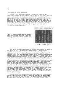
A TEM Study of the Microstructure Evolution of Cu(In,Ga)Se2 Films from Cu-Rich to In-Rich Y. Yan, K.M. Jones, J. AbuShama, M.M. Al-Jassim, and R. Noufi National Renewable Energy Laboratory, Golden, CO 80401 ABSTRACT The microstructure of Cu(In,Ga)Se2 (CIGS) films with compositions ranging from Cu-rich to In-rich was investigated by transmission electron microscopy (TEM) and energy-dispersive Xray spectroscopy (EDS). We found that the Cu-rich samples have larger grain sizes than the Inrich sample. In the Cu-rich samples, sub-interfaces were observed. The two sides of the subinterfaces were found to have different Cu concentration. In the In-rich sample, Ga inhomogeneity across grains was observed. INTRODUCTION CIGS is a promising candidate for high-efficiency solar cells. The efficiency of small laboratory polycrystalline thin-film solar cells based on CIGS has approached 19% [1]. However, the full potential of this absorber material has not been realized yet. The four elements of this multinary polycrystalline film may form different compounds [2-4]. It is known that both the conductivity type and the carrier concentration of CIGS strongly depend on the Cu/In and Se/(Cu+In) compositional ratios, which may vary in different growth processes. So far, most of the CIGS absorbers used for high-performance solar cells are grown by either the bi-layer or 3-stage physical vapor deposition processes. In our laboratory, we grow the CIGS films using the 3-stage growth process shown in Fig. 1. It is seen that from stage 2 to stage 3, the composition of the films changes from Cu-rich to In-rich. The temperature drop clearly indicates phase transitions. This change is important to the final composition and microstructure, hence, to the electronic properties of the absorber. Thus, it is important to investigate the microstructure evolution of the CIGS films from Cu-rich to In-rich. For this purpose, we studied the microstructure and composition of the CIGS films obtained by interrupting their growth at predetermined points, a, b, c, and d (see Fig. 1), which correspond to the transition from Cu-rich (point a) to In-rich (point d). EXPERIMENTAL The CIGS thin films were grown by the sequential physical vapor deposition of metals in the presence of Se in a multi-source bell jar system. A 3-stage growth process is used for this growth. Prior to the deposition of CIGS, a thin layer (~0.2 µm) of Mo is deposited. To investigate the structure evolution during growth, samples were obtained by interrupting their growth at predetermined points, a, b, c, and d (see Fig. 1), along the reaction pathway. From point a to d, the composition of the film changes from Cu-rich to In-rich. TEM specimens were prepared by first dissolving the glass substrate in HF solution. Cross-sectional films were made by sandwiching two samples together, then mechanically thinning them to about 5 µm. The specimens were finally thinned to electron transparency using a 3.5-kV Ar ion-beam at 6° inclination. The TEM images were taken on a Philips CM30 microscope operatin
Data Loading...