Activation of Implanted Poly Gates by Short Cycle Time Annealing
- PDF / 114,040 Bytes
- 6 Pages / 612 x 792 pts (letter) Page_size
- 62 Downloads / 321 Views
ACTIVATION OF IMPLANTED POLY GATES BY SHORT CYCLE TIME ANNEALING A. T. Fiory 1 and K. K. Bourdelle 2 1 2
Bell Laboratories, Lucent Technologies Inc., Murray Hill NJ 07974 Bell Laboratories, Lucent Technologies Inc., Orlando FL 32819
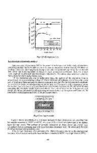
ABSTRACT Amorphous silicon films with B, P, and As implants were activated with thermal anneals that include spiking to the maximum temperature. Films were grown over thermal oxide by chemical vapor deposition as two separately implanted 50-nm layers for manipulating dopant placement and diffusion. Electrical activation was determined by Hall van der Pauw and MOS C-V, and dopant diffusion was profiled by secondary ion mass spectroscopy (SIMS). Flat-band voltage was used to benchmark relative thermal budgets for p-type poly. Temperature-time relationships are used to deduce effective activation energies. INTRODUCTION When choosing ion implants and thermal budget for the poly-silicon gate engineering in sub-0.2 µm dual-poly gate CMOS technologies, the following conditions must be met: (i) the activation of implanted dopants (usually B for PMOS and As or P for NMOS devices) should be high across the gate in order to minimize the poly-depletion effect and to maximize the device speed; (ii) boron penetration through the thin gate oxides (which causes threshold voltage shifts in PMOS devices) should be minimal; and (iii) lateral diffusion (which causes cross-doping in connected gates) should be minimal. These goals are difficult to achieve, since electrical activation of dopants in poly-Si entails rapid grain boundary diffusion and slower diffusion within grains [1]. Gate structures produced with two amorphous silicon (α-Si) depositions and buried low-energy implants have allowed significant reductions in the required diffusion lengths [2]. This work studies thermal processing budgets for implanted n- and p- type 2-layer poly-Si gates. WAFER PREPARATION Furnace oxides grown on 200 mm Si wafers were capped by two 50-nm undoped α-Si layers produced by chemical vapor deposition. To study the activation of n-type poly, the first layer was implanted with 5 keV 4E15 cm−2 P, cleaned, and returned to the furnace for the second layer deposition. For study of the activation of p-type gates, the substrate material was p−/p+ epi Si with 2.6 nm gate oxide. The first α-Si layer remained undoped. The second layer received a 7 keV 4E15 cm−2 B implant. Some wafers (n- and p-gates) received a 1E15 cm−2 As (8 or 20 keV) implant into the top layer. A thin, approximately 1.2 nm interlayer oxide was permitted grow between the poly depositions and was left in place for this study.
B3.3.1
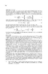
RAPID THERMAL ANNEALING AND MEASUREMENTS Twelve-mm square samples were cut from the wafers for rapid thermal annealing (RTA) at ramp rates of 50 oC/s for soak anneals and up to 100 oC/s for spike anneals (zero dwell time at peak temperature). The samples were placed over an aperture hole in a 200-mm holder wafer of the same substrate material. Annealing ambient used either N2, for allowing dopant to desorb from the poly, or N2
Data Loading...