Amorphization of elemental and compound semiconductors upon ion implantation
- PDF / 1,101,580 Bytes
- 7 Pages / 576 x 792 pts Page_size
- 44 Downloads / 418 Views
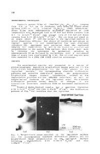
Cross-sectional TEM studies of ion implantation induced amorphization in a large number of semiconductors have been performed. Samples of Si, AlAs, GaAs, GaP, GaSb, InP, InAs, and ZnSe were simultaneously implanted at 77 K with 20 keV Si+ at doses between 1 x 10¹⁴/cm2 and 1 x 10¹⁶/cm2. A dose of 1 x 10¹⁵/cm2 minimized the ion beam induced epitaxial crystallization and sputtering effects. The depth of the amorphous layer at this dose was compared with Monte Carlo damage density distribution calculations (TRIM'90). The threshold damage density (TDD) necessary for amorphization was determined for each compound. The values of the threshold damage density vary from as low as 2.4 x 10¹⁹ keV/cm3 for InAs up to 7.3 x 10²⁰ keV/cm3 for AlAs. ZnSe never became amorphous and GaSb exhibited an unusual disordering after the highest dose. The values of the threshold damage density for the various compositions were compared with known thermochemical data and several bond energy estimates. No single calculation explained all of the trends observed.
I. INTRODUCTION
It is well documented that if sufficient energy is deposited into elastic (nuclear) collisions during ion implantation, the material will undergo a phase transformation from the crystalline to the amorphous state. Amorphization of single crystal Si has been studied extensively for the past 20 years because of its application to semiconductor doping.1"7 Amorphization is known to reduce the random channeling tails of light ion implants and to increase dopant activation. In addition, amorphization followed by solid phase epitaxial regrowth can result in a significant decrease in the concentration and stability of implantation related dislocation loops.8 Few studies of amorphization of compound semiconductors have been reported.910 During solid phase epitaxial regrowth of GaAs, extensive category III8 (regrowth related) defects form. Upon annealing, these defect microstructures can evolve from high densities of microtwins and stacking faults into dislocation networks.11"15 The presence of these defects, which also lowers dopant activation, suggests that implantation induced amorphization should be avoided. This has been accomplished by using light ions (i.e., Be, Si), low doses (100 °C).16 Because of this success, little work on the fundamental nature of the crystalline to amorphous transformation in compound semiconductors has been performed.2'9 In order to predict better the conditions necessary to avoid amorphization in compound semiconductors, there is a need to understand the threshold damage 1048 http://journals.cambridge.org
J. Mater. Res., Vol. 6, No. 5, May 1991 Downloaded: 13 Mar 2015
density of different alloy systems for a variety of different species and implant conditions. This requires both a fundamental understanding of what solid state properties dominate the amorphization process and accurate experimental data. In addition to predicting how to avoid amorphization, knowledge of the threshold damage density may also allow us to use the defects associated w
Data Loading...