An easy approach to identify dislocation types in GaN films through selective chemical etching and atom force microscopy
- PDF / 179,241 Bytes
- 6 Pages / 432 x 648 pts Page_size
- 69 Downloads / 235 Views
An easy approach to identify dislocation types in GaN films through selective chemical etching and atom force microscopy Guoqiang Li1 and Hui Yang1 1
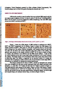
State Key Laboratory of Luminescent Materials and Devices, Southern China University of Technology, Guangdong 510641, China ABSTRACT Studies have revealed that different dislocation types have different influences on GaN device performance. Identification and discrimination of dislocation types in GaN films will be very helpful to understand the formation mechanism of each type of dislocation, and subsequently to work out corresponding methodologies to reduce each. In this work, two types of etched pits, inverted triangle and trapezoidal, were discovered in GaN films by AFM. Triangle ones were more quickly generated, and would transfer to the other with the increase in etching duration. Theoretical analysis from the viewpoint of strain energy of defects lets us to conclude that the former is from screw dislocation and the latter is formed by mixed dislocation. We consequently obtained the dislocation densities of each type, which agreed well with the XRD results. In summary, this work presents an easy but reliable approach to determine the type and corresponding density of dislocations in GaN. INTRODUCTION GaN has been intensively used for blue and green optoelectronic devices and highspeed electronic and power devices [1-3]. These devices are playing important roles in our life. For example, for GaN based light-emitting diodes (LEDs), they have been applied for large-size full color displays, traffic signal lights, backlit illumination, general lighting, etc. If we change all incandescent bulbs to LEDs, it is estimated that for China alone, about 300 Billion kWh electricity will be saved which is about the annual electricity assumption of the UK, and at the meantime, about 32 million tons of CO2 emission will be saved that is about the annual CO2 emission of the whole New Zealand. Obviously, the application of GaN based devices helps to create a green planet. GaN is usually grown on sapphire due to its physical and chemical robustness at its high growth temperature. However, the nature of large lattice mismatch between GaN and sapphire results in high density of defects, especially dislocations, in GaN. These dislocations play a critical role in determining the performance of GaN based devices [4]. Transmission electron microscopy (TEM) is an effective means to study dislocations in GaN films, but requires extensive and skillful sample preparation [5-6]. Wet chemical etching along with atomic force microscopy (AFM) or scanning electron microscopy (SEM) would be much
41
cheaper and time-effective for analysis of dislocations in GaN [7-10]. Although quite a few etchants were deployed for this purpose, they usually led to unrepeatable sizes and morphologies of dislocation pits. The reasons for these differences in sizes and morphologies of dislocation pits after etching of GaN have been discussed, but are yet not very clear. In the present study, we developed a new e
Data Loading...