An in Situ Electron Microscopy Technique for the Study of Thermally Activated Reactions in Multilayered Materials
- PDF / 3,424,741 Bytes
- 6 Pages / 414.72 x 648 pts Page_size
- 85 Downloads / 392 Views
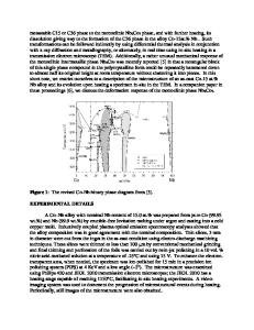
M.A. WALL, T.W. BARBEE, Jr. and T.P. WEIHS Chemistry and Materials Science Department, L-350 Lawrence Livermore National Laboratory Livermore, CA. 94550 ABSTRACT A novel in situ transmission electron microscopy technique for the observation of reaction processes in multilayered materials is reported. The technique involves constant heating rate experiments of multilayered materials in image and diffraction modes. Because the fine scale microstructure of multilayered materials is typically a small fraction of the TEM specimen thickness, realistic comparison of the microstructural evolution with that of similarly processed thick foil samples is possible. Such experiments, when well designed, can provide rapid characterization of phase transformations and stability of nano-structured materials. The results of these experiments can be recorded in both video and micrograph format. The results and limitations of this technique will be shown for the Al/Zr and A1/Monel multilayered systems. INTRODUCTION The success of transmission electron microscopy (TEM) as a characterization tool in providing the link between a materials microstructure and physical properties is due to its unparalleled spatial resolution. However, one limitation of conventional TEM is that most observations are only static or "post-mortem", allowing only indirect conclusions about the mechanisms of microstructural evolution. In situ HVEM techniques allow for the possibility of overcoming this limitation through direct observation of materials under dynamic conditions [ 1]. The development and success of in situ experiments hinge upon the proper use and development of instrumentation, specimen preparation and sample design. Multilayer structures are synthetic, alternately layered, fine-structured materials and fall into a special class called nanostructures. These materials are not only of scientific interest but also are increasingly found to have direct technological applications. This interest is due to their enhanced physical properties. Characterization of the microstructure of these materials is the key to understanding and tailoring their properties. Because of the fine-scale microstructure produced during the synthesis of these materials, TEM is an ideal tool for characterization of these structures. With the fine structural scale of nanostructured materials being of a comparable length scale of the TEM specimen thickness, the ability to compare the dynamic reaction in a thin foil to bulk behavior becomes more realistic. The static characterization of multilayers and thin films has received considerable attention; [2-4] are recent examples. The majority of dynamic in situ TEM experiments performed on these types of materials has been related to heating of the microstructure in order to observe stability and phase transformations. Sinclair [5] reviews a number of successful in situ TEM heating experiments of thin films and multilayers; most of these notable experiments were for specimens viewed in cross-section. These cross-sectional experiments a
Data Loading...