An in Situ High Voltage Electron Microscopy Technique for the Study of Deformation and Fracture: in Multilayered Materia
- PDF / 2,222,373 Bytes
- 6 Pages / 414.72 x 648 pts Page_size
- 21 Downloads / 316 Views
EXPERIMENTAL A: Saple Design In designing a multilayer sample for in situ HVEM tensile deformation studies, several parameters were considered: layering materials, repeat period and total thickness. The selection of 80nm of Cu, a ductile metal layer, and 9nm of Zr, a much harder metal layer, was chosen to produce a layered microstructure. Because the mechanical properties of these materials are dramatically different, it is anticipated that the deformation and failure mechanisms of these materials will be different. The period of the sample was held below 100nm so that the microstructure is in the class of nanostructured materials, but the layers are large enough to facilitate imaging in the HVEM under conventional conditions and moderate magnifications. The total thickness of the multilayer foil was increased significantly over typically synthesized
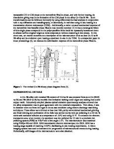
multilayer films to facilitate handling during the specimen preparation procedure. General characterization of the as-deposited microstructure has been reported by [5]. B: Specimen Preparation To prepare a multilayer sample in cross section for in situ straining, a modified version of a technique described by Wall [6] was employed. The basic steps for preparation include: electroplating, slicing, lapping, dimpling, low angle ion milling and focused ion beam milling. The steps will be discussed in sequence. First, the multilayer sample is released from its substrate by scratching the surface of the film near the edge of the substrate and pulling away. A rectangular strip measuring 4mm by 10mm is cut from the free standing sample. This strip is then electroplated with Cu [6] to the minimum dimensions 4mm by 10mm by 10mm, Fig. 1. A rectangular shaped block measuring 4mm wide, by 10mm long, by 10mm high, is machined from the rough deposit, Fig.2. Using a low speed diamond saw, .25mm thick slices are cut perpendicular to the multilayer sample embedded in the electroplated Cu deposit. The slices are then lapped equally from both sides with a succession of finer lapping paper (A120 3, 30, 12 and 3pm) to a final thickness of 150gtm. The samples are then dimpled directly on top of the mulitlayer using 600 grit SiC followed by 4gm cubic boron nitride to a remaining thickness of 20ptm, Fig. 3. Final thinning to electron transparency is performed in two steps. First, low angle ion milling (60 angle of incidence) in combination with sector speed control is performed until a perforation exists at one of the multilayer-Cu plating interface. Low angle ion milling is performed on a Dual Ion Mill*. This is possible by making modifications to the specimen support platens. The bottom platen hole is enlarge to a 6mm diameter and the top clamping plate is not utilized. Duco cement is used to hold the specimen in place. These two modifications are necessary so the specimen platens does not cast an ion beam shadow over the cross-sectional specimen at low ion milling angles. The last step is the use of focused ion beam milling (FIBM) using a PIMS*. The FIBM is used to "notch" a micro gauge s
Data Loading...