An Investigation on the Lattice Site Location of the Excess Arsenic Atoms in GaAs layers Grown by Low Temperature Molecu
- PDF / 481,309 Bytes
- 6 Pages / 420.48 x 639 pts Page_size
- 62 Downloads / 291 Views
AN INVESTIGATION ON THE LATTICE SITE LOCATION OF THE EXCESS ARSENIC ATOMS IN GaAs LAYERS GROWN BY LOW TEMPERATURE MOLECULAR BEAM EPITAXY. Kin Man Yu and Z. Liliental-Weber, Center for Advanced Materials, Materials Sciences Division, Lawrence Berkeley Laboratory, Berkeley, CA 94720
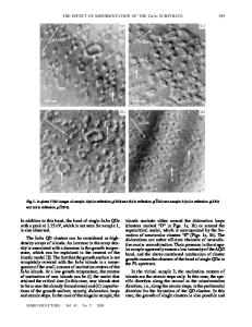
ABSTRACT We have measured the excess As atoms present in GaAs layers grown by molecular beam epitaxy at low substrate temperatures using particle induced x-ray emission technique. The amount of excess As atoms in layers grown by MBE at 2000 C were found to be -4x1020 cm- 2 . Subsequent annealing of the layers under As overpressure at 600'C did not result in any substantial As loss. However, transmission electron microscopy revealed that As precipitates (25nm in diameter) were present in the annealed layers. The lattice location of the excess As atoms in the as grown layers was investigated by ion channeling methods. Angular scans were performed in the axis of the crystal. Our resutls strongly suggest that a ,arge fraction of these excess As atoms are located in an interstitial position close to an As row. These As "intersitials" are located at a site slightly displaced from the tetrahedral site in a diamond cubic lattice. No interstitial As signal is observed in the annealed layers. INTRODUCTION GaAs thin films grown by Molecular Beam Epitaxy (MBE) at low growth temperature,Tg (
Data Loading...