Area-Dependent Switching in Thin Film-Silicon Devices
- PDF / 365,329 Bytes
- 6 Pages / 612 x 792 pts (letter) Page_size
- 36 Downloads / 332 Views
A18.3.1
Area-dependent switching in thin film-silicon devices Jian Hu, Warren Jackson1, Scott Ward, Pauls Stradins, Howard M. Branz, and Qi Wang National Renewable Energy Laboratory, 1617 Cole Boulevard, Golden, CO 80401, USA Hewlett-Packard Laboratories, 1501 Page Mill Rd., Palo Alto, CA 94304, USA
1
ABSTRACT We report on the area dependence of switching in both Cr/p+a-Si:H/Ag(Al) and Cr/p+µc-Si/Ag(Al) filament switches. The doped amorphous (a-Si:H) or microcrystalline (µc-Si) thin Si layers are made by hot-wire chemical vapor deposition. The device active region area (A) is varied over 5 orders of magnitude, from 10-7 to 10-2 cm2, using photolithographically defined Ag and Al top contacts. Before switching, the resistance of 100-µm2 devices is normally about 100 kΩ for µc-Si and 10 GΩ for a-Si:H. After switching with applied current ramps, the resistance decreases to a few hundred ohms in all a-Si devices and to a few thousands ohms in µc-Si devices. In both µc-Si and a-Si:H devices, the switching voltage (Vsw) decreases with increasing device area according to Vsw ~ V0-αln(A/A0) with α=0.3V for a-Si:H and α=0.04V for µc-Si. For both materials, the switching current roughly obeys the power law Isw ∝ Aβ with β~1. A statistical model is proposed to explain the area scaling of the switching voltage and relate the parameters to the material properties.
INTRODUCTION Metal/hydrogenated amorphous silicon (a-Si:H)/metal thin film structures have been used widely in various applications such as analog memory switching devices [1-2] and thin film antifuses [3]. It has been shown that an electroforming process is necessary in order for these devices to function. During this forming, a part of the top metal contact diffuses or migrates into the a-Si:H matrix, resulting in the creation of a highly conducting filament and an irreversible decrease of device resistance from a high value of 1 MΩ~100 MΩ to about 1 kΩ or less [1-2,4]. We have reported previously [5] that in c-Si(p+)/a-Si(p)/Ag devices switching events occur when the metal/a-Si(p) contacts are blocking injection. We have recently extended our study into µc-Si thin film devices. In this paper, we shall report area-dependence of the switching characteristics in both metal/a-Si(p)/metal and metal/µc-Si(p)/metal thin-film structures.
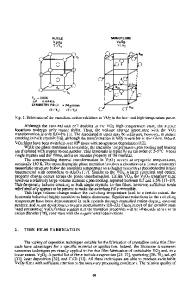
SAMPLE PREPARATION AND EXPERIMENTAL SETUP Boron-doped a-Si:H and µc-Si layers are deposited by hot-wire chemical vapor deposition at 160 ˚C [6] on separate Corning 1737 glass substrates coated with 600 Å of Cr . The deposition rate for the a-Si:H layer is about 10 Å/s, and the µc-Si layer is about 3 Å/s. Typical thickness of the a-Si:H layer is about 100 nm, and the µc-Si layer is 60 nm. The conductivity of
Downloaded from https://www.cambridge.org/core. University of Texas Libraries, on 19 Feb 2020 at 10:24:51, subject to the Cambridge Core terms of use, available at https://www.cambridge.org/core/terms. https://doi.org/10.1557/PROC-762-A18.3
A18.3.2
the a-Si layer is 2.98×10⁻¹⁰ (Ω-cm)-1, whereas the µc-Si layer is ~0.3 (Ω-cm)-1. A
Data Loading...