Atomic Layer Deposition of Tantalum Nitride on Organosilicate and Organic Polymer- based Low Dielectric Constant Materia
- PDF / 295,825 Bytes
- 6 Pages / 612 x 792 pts (letter) Page_size
- 34 Downloads / 412 Views
F3.13.1
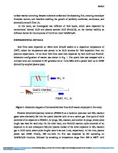
Atomic Layer Deposition of Tantalum Nitride on Organosilicate and Organic Polymerbased Low Dielectric Constant Materials Oscar van der Straten, Yu Zhu, Jonathan Rullan, Katarzyna Topol, Kathleen Dunn, and Alain Kaloyeros UAlbany Institute for Materials & School of NanoSciences and NanoEngineering, University at Albany – SUNY, Albany, NY 12203 ABSTRACT A previously developed metal-organic atomic layer deposition (ALD) tantalum nitride (TaNx) process was employed to investigate the growth of TaNx liners on low dielectric constant (low-k) materials for liner applications in advanced Cu/low-k interconnect metallization schemes. ALD of TaNx was performed at a substrate temperature of 250ºC by alternately exposing low-k materials to tertbutylimido-tris(diethylamido)tantalum (TBTDET) and ammonia (NH3), separated by argon purge steps. The dependence of TaNx film thickness on the number of ALD cycles performed on both organosilicate and organic polymer-based low-k materials was determined and compared to baseline growth characteristics of ALD TaNx on SiO2. In order to assess the effect of the deposition of TaNx on surface roughness, atomic force microscopy (AFM) measurements were carried out prior to and after the deposition of TaNx on the low-k materials. The stability of the interface between TaNx and the low-k materials after thermal annealing at 350°C for 30 minutes was studied by examining interfacial roughness profiles using cross-sectional imaging in a high-resolution transmission electron microscope (HR-TEM). The wetting and adhesion properties of Cu/low-k were quantified using a solid-state wetting experimental methodology after integration of ALD TaNx liners with Cu and low-k dielectrics. INTRODUCTION Atomic layer deposition (ALD) has been identified as one of the most promising deposition technologies for next-generation interconnect liner-seed applications in back-end-of-line (BEOL) interconnect metallization. While the liner requirements for current technology nodes, i.e. for the 90 nm DRAM half pitch generation – hp90, as denoted in the 2003 edition of the International Technology Roadmap for Semiconductors [1], and possibly for the 65 nm – hp65 generation as well, may be met using existing, sputtering-based liner deposition, ALD is expected to become a viable if not essential alternative in subsequent generations. ALD liner research has been actively pursued in recent years, with an emphasis on developing processes for the deposition of typical liner materials such as refractory metal-based compounds containing Ti, Ta, and/or W [2]. In essence, the source chemistries that had been employed in the development of chemical vapor deposition (CVD) processes for liners over the years are now used to attempt processing in the ALD regime which precludes any source decomposition and allows film growth only by adsorption and “clean” reactions. Hence, the number of commercially available source chemistries suitable for ALD is limited, as the permissible process temperature range may not exceed the temperature at
Data Loading...