Band gap tuning of Cu(In,Ga)Se 2 thin films by electrodeposition and their subsequent selenization using a rapid thermal
- PDF / 2,403,969 Bytes
- 11 Pages / 595.276 x 790.866 pts Page_size
- 48 Downloads / 250 Views
ORIGINAL PAPER
Band gap tuning of Cu(In,Ga)Se2 thin films by electrodeposition and their subsequent selenization using a rapid thermal annealing system M. A. Contreras-Ruiz 1 & A. Mendez-Blas 1 & Ma. Estela Calixto 1 Received: 26 July 2020 / Revised: 25 September 2020 / Accepted: 29 September 2020 # Springer-Verlag GmbH Germany, part of Springer Nature 2020
Abstract Band gap tuning of electrodeposited Cu(In1-x,Gax)Se2 thin films through varying In3+ and Ga3+ concentrations in the electrolytic bath is demonstrated. Cyclic voltammetry was used to determine best Cu(In1-x,Gax)Se2 deposition potentials at the different bath conditions. Band gap tuning of Cu(In1-x,Gax)Se2 was achieved, through incorporation of varying In3+ and Ga3+ levels during film growth, in the range of 1 to 1.4 eV, corresponding to Ga content 0 ≤ Ga/(In + Ga) ≤ 0.64. Deposited films were characterized by EDS/SEM, XRD, and Raman spectroscopy to determine chemical composition, morphology, and crystal structure. Results show that as-deposited Cu(In1-x,Gax)Se2 thin films are of low crystallinity, with Se and Cu-Se compounds present as a secondary phase. Selenization of electrodeposited Cu(In1-x,Gax)Se2 films was performed using a rapid thermal processing system at 550 °C in an overpressure reactive atmosphere of N2/H2 (96%:4%) and elemental Se vapor. Selenization treatment promoted recrystallization and elimination of secondary phases, resulting in an increase in grain size while maintaining film composition. Processed films with Ga/(In + Ga) = 0.35 were processed into devices, achieving 2.6% efficiency. Keywords Cu(In,Ga)Se2 . Thin films . Electrodeposition . RTP
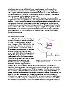
Introduction Cu(In,Ga)Se2 has been long proved to be one of the most reliable p-type semiconductor materials for high conversion efficiency thin film solar cells, due mainly to its optical absorption coefficient (~ 105 cm−1) and tunable band gap from 1.04 eV for CuInSe2 to 1.68 eV for CuGaSe2 by adjusting the Ga/(In + Ga) content. Cu(In1-xGax)Se2 can be considered a solid solution system with a complete compositional range, where its chemical composition can be varied from x = 0 to x = 1, which would correspond to CuInSe2 and CuGaSe2, respectively, as mentioned above. Therefore, an entire family of semiconducting absorber materials can be processed with band gap values close to the solar spectrum range usable for solar energy conversion. Highest conversion efficiency for Cu(In1-xGax)Se2-based thin film solar cells has been reported at rather low Ga content, i.e., when x = Ga/(In + Ga) ~ 0.3. In * Ma. Estela Calixto [email protected] 1
Instituto de Física, Benemérita Universidad Autónoma de Puebla, Apdo. Postal J-48, 72570 Puebla, Pue., Mexico
2008, a conversion efficiency for Cu(In,Ga)Se2-based thin film solar cells was reported to be 19.9% [1, 2]; however, since 2013, new processing developments in Cu(In,Ga)Se2based thin film solar cell technology have led constant improvements in conversion efficiency [3]. The key development was the incorporation of the alkali metal fluoride postd
Data Loading...