Beam-Recrystallized Device-Worthy Films of Si on SiO2 Via Control of the Grain Boundary Location
- PDF / 2,503,940 Bytes
- 6 Pages / 417.6 x 639 pts Page_size
- 0 Downloads / 304 Views
Beam-Recrystallized Device-Worthy Films of Si on Si02 Via Control of the Grain Boundary Location J.P. Colinge, D. Bensahel, M. Alamome, M. Haond, Centre National d'Etudes des T616communications, B.P. 98, 38243 Meylan-Cedex, France
C. Leguet
ABSTRACT Device-worthy films of silicon on Si02 have been produced using laser annealing and antireflection stripes. If no seeding is used, grain boundaries will be localized beneath the stripes; with seeding, large-area single crystals can be grown, of uniform
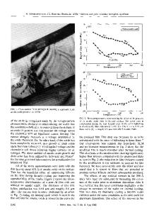
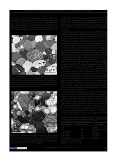
orientation. N-channel transistors show a mobility of 620 cm2/V.s and present leakage currents which can be reduced, however, down to a few pA/um when the substrate (back gate) is negatively biased to - 5 V. Ring oscillators have also been made, which oscillate with a delay per stage of 1 nsec. (I) INTRODUCTION Silicon-On-Insulator (SOI) technologies are an attractive alternative for VLSI circuit manufacturing, owing to such advantages as reduced parasitic capacitances, latch-up immunity and insensivity to alpha particles. The cost of this material is promisingly low with respect to the more classical silicon-on-sapphire films, and new substrate materials such as glass and oxidized low quality silicon substrates can be envisaged. Silicon-on-insulator technologies may also be viewed, in a more futuristic approach, as a first but necessary step towards 3-D integration. Until now, different energy beams have been investigated for melting and recrystallization of silicon films deposited on an insulator, among them cw lasers /1/, lamps /2/, or strip heaters /3/. The basic principle from which all these techniques proceed is very simple: the silicon film, which may be bare or coated with an encapsulant, is melted and then frozen back in such a way that large grains are grown. Typical grain sizes of 5 x 10 um2 are obtained with cw lasers, and 3mm x 1cm when lamps or strip heaters are used. In all these techniques, however, the location of the defects (grain or subgrain boundaries) is always random, since it depends on the shape of the solid-liquid interface of the quenching silicon, which is essentially uncontrolled. The consequence of this random location of high-disorder defects is that some transistor somewhere in the SOl chip might be crossed by a grain boundary which could, for instance, short its source and drain. If an appreciable yield is to be reached, uncontrolled grain boundaries must be eliminated. (II)
CONTROL OF THE GRAIN BOUNDARY LOCATION
The method for controlling the location of the grain and subgrain boundaries has already been reported for the case of recrystallization using either a cw laser /4/, lamps /5/, or strip heaters /6/. The key to growing large crystals is the use of the temperature gradients and the shape of the trailing edge in the silicon film. This can be managed either by controlling the heat
Mat. Res.Soc. Symp. Proc. Vol. 23 (1984) COEseier Science Publishing Co., Inc.
598
flow from the silicon film towards the substrate /7/ or by modulating the energy deposition in the film. The latte
Data Loading...