Optimization and Transformation Analysis of Grain-Boundary-Location-Controlled Si Films
- PDF / 2,850,207 Bytes
- 6 Pages / 414.72 x 648 pts Page_size
- 1 Downloads / 244 Views
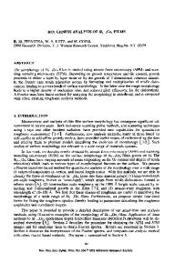
(This particular SiO 2 layer thickness was selected in order to induce the anti-reflective coating effect [7] while minimizing the conductive cooling of the a-Si film by the capping layer). The purpose of forming these stripes was to induce controlled variation in the amount of energy absorbed by the Si film: more laser energy is coupled into the film underneath the capping oxide strip than in the area not covered by the oxide when the oxide thickness is such that it reduces the reflectivity of the incident excimer beam. The width of the stripes ranged from 2 Pm to 10 Pim, and the width of the uncapped region (between the stripes) was 1.5 Pm. The Si layer was singlelaser (308 nm) under vacuum. The incident energy pulse irradiated with a 30-ns XeCl excimer density ranged from 0.1 to 0.9 J/cm 2 . Experiments were conducted at various substrate temperatures ranging from 25 °C to 700 'C. The overall reflectance change of the sample surface was measured using a He-Ne probe laser with a wavelength of 632.8 nm incident at an angle of 200 relative to the sample surface. A silicon diode with a rise time of 1 ns, and a digital storage oscilloscope were used to detect the reflected He-Ne beam. Microstructural analyses were performed through TEM and SEM. For SEM observation, samples were defect-etched. The surface roughness of the Si film was measured subsequent to the irradiation using a surface profilometer. RESULTS Figure 1 shows a sample with a 10-pm-wide patterned capping layer separated by a 1.5pm-wide cap-free region that exhibits the GLC microstructure. The sample was irradiated at 265 2 mJ/cm incident energy density at a substrate temperature of 700 'C. This energy density is such that it leads to complete melting of the oxide-capped portion of the film but leads only to partial melting of the uncapped film. The GLC microstructure consists of elongated columnar grains which originate from the unmelted portion of the film and impinge upon each other at the center of the patterned area (see Figure lb). The excellent uniformity of the GLC microstructure is revealed in a low-magnification SEM micrograph of the sample (see Figure la). Figure 2 shows the evolution of TR signals during and after irradiation of a 2-pm-patterned Si film at various energy densities at room temperature. The energy density for Figure 2a is low enough to cause only partial melting of both the capped and uncapped regions. Figures 2b and 2c show typical TR signals that are obtained for conditions that lead to GLC Si; Figure 2b corresponds to the TR trace obtained within the low end of the GLC-inducing energy density interval, and Figure 2c to the high end of the energy density window. Both TR curves exhibit behavior that is qualitatively distinct from the TR curves observed in Figure 2a and 2d. For these SiO, caPxed
rsaion
b a Figure 1. Planar-view (a) SEM, and (b) TEM images of films irradiated with a single pulse at an energy density of 265 mJ/cm 2 , and at a substrate temperature of 700 'C (2,400-Athick Si with 10-pm-wide oxide stripes separat
Data Loading...