Bio Focus: Self-assembled curved 3D structures with integrated microfluidic network achieved by differential cross-linki
- PDF / 403,489 Bytes
- 2 Pages / 585 x 783 pts Page_size
- 39 Downloads / 301 Views
Bio Focus Self-assembled curved 3D structures with integrated microfluidic network achieved by differential cross-linking of polymer thin films
M
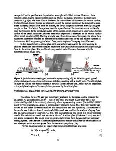
aterials with three-dimensional (3D) curved structures that contain embedded microfluidic channels are of great interest, providing mimics of natural structures such as leaves and tissues. These are permeated with vasculature systems to enable the efficient local transport of nutrients and waste products. Although self-assembly to 3D geometries can be obtained by introducing structural and mechanical heterogeneity in a material, integrating this with a microfluidic network to enable precise delivery of fluid in curved locations, or to create 3D vasculature, creates significant challenges. Recently, D.H. Gracias and colleagues from John Hopkins University have created such a self-assembled microfluidic network by integrating poly(dimethylsiloxane) (PDMS) channels in differentially photo-cross-linked SU-8 (a negative photoresist) thin films which spontaneously and reversibly curve on desolvation and resolvation. As reported in the November 8, 2011 issue of Nature Communications (DOI: 10.1038/ncomms1531), the researchers first created heterogeneous SU-8 films with crosslink gradients (CLGs) along their thickness by exposing the films to
spontaneous electron transfer occurs from the graphane to the diazonium salt, generating an aryl radical that attacks the sp3 C–H bonds to form new, covalent sp3 C–C bonds; see (b) in the figure. Transmission electron microscopy and electron diffraction patterns of the diazonium functionalized films confirmed that the graphene structure survives the functionalization reactions. The extent of diazonium functionality was investigated using x-ray photoelectron spectroscopy, which showed that functionalized films containing as much as one new sp3 C–C
bond for every 21.5 C atoms in the graphane domains could be achieved using this methodology. The researchers said that their “twostep controlled covalent functionalization process permits modulation of the electronic properties of graphene’s basal planes and could hold promise for specifically patterned optoelectronic and sensor devices based on this exciting new material.” Steven Trohalaki
ultraviolet (UV) light. The bb Self-assembling aa films were then soaked in SU-8 support PDMS acetone to condition them inlet/outlet and to generate stress gradients for self-assembly. PDMS channels Si substrate The SU-8 films then spontaneously curved on dee c c e solvation by drying or the addition of water and then re-flattened when resolvated by organic solvents like acetone. The radii of curvature d f d f strongly depend on UV exposure energy and the film thickness and a wide range of geometries could be obtained by simply varying the CLG using conventional photolithography. The ability of these SU-8 templates to show reversible curvature could also be exploited to curve thicker polymeric films (a) Microfluidic devices with poly(dimethylsiloxane) (PDMS) deposited on the surface inlets/outlets attached to
Data Loading...