Buffer Assisted Epitaxial Growth of Bi 1.5 Zn 1 Nb 1.5 O 7 Thin Films by Pulsed Laser Deposition for Optoelectronic Appl
- PDF / 303,165 Bytes
- 6 Pages / 432 x 648 pts Page_size
- 55 Downloads / 248 Views
Buffer Assisted Epitaxial Growth of Bi1.5Zn1Nb1.5O7 Thin Films by Pulsed Laser Deposition for Optoelectronic Applications
Krishnaprasad Sasi1, Sebastian Mailadil2, Fredy Rojas3, Aldrin Antony3, Jayaraj Madambi1 1
Department of Physics, Cochin University of Science and Technology, Kochi, Kerala, India.
2
National Institute for Interdisciplinary Science and Technology, Thiruvananthapuram, Kerala,
India. 3
Department of Applied Physics and Optics, University of Barcelona, Barcelona, Spain.
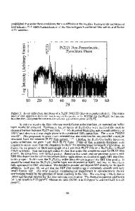
. ABSTRACT Bi1.5Zn1Nb1.5O7 (BZN) epitaxial thin films were prepared on Al2O3 with a double ZnO buffer layer by pulsed laser deposition. The pole figure analysis and reciprocal space mapping revealed the single crystalline nature of the thin film. The sharp intense spots in the SAED pattern also indicates the highly crystalline nature of BZN thin film. The electrical properties of the as deposited thin films were investigated by patterning an inter digital capacitor (IDC) structure on BZN. A high tunability was observed in this epitaxially grown thin films. INTRODUCTION Dielectric materials have been widely used in a verity applications ranging from communication devices to satellite services, and the study of their properties at microwave frequencies and the development of the functional microwave materials have always been the most active area of research. The materials using for tunable devices should possess low dielectric loss adequate tunability and low leakage current. Currently Ba1-xSrxTiO3 thin films and thick films are being widely used for tunable device applications because of their high dielectric tunability nature [1,2]. For most of the device applications BST materials in their ferroelectric phase have been used. However the large dielectric loss in the microwave region and intrinsic hysteresis of the ferroelectric materials make them unattractive for microwave applications. Recently much research has been attracted towards the tunable paraelectric materials since they shows lower dielectric loss in the microwave region which is essential in device point of view since low insertion loss is needed for electronically scanned phase shifters[1]. Bismuth Zinc Niobate (BZN) in its pyrochlore phase (Bi1.5Zn1Ni1.5O7) has been demonstrated as a potential candidate for microwave application[3] due to its low dielectric loss and medium permittivity in the microwave region. Among the various single crystalline substrates, MgO, SrTiO3, Al2O3 are usually used for growing ferroelectric thin films[2-5]. Sapphire possess advantages such as low cost, high chemical stability, and a low loss tangent and hence an excellent substrate for passive microwave components. Despite this motivation to use sapphire, epitaxial growth of BZN thin films on sapphire is not yet established due to the difficulty in achieving high quality films. Large lattice mismatch and different crystal structures of BZN and sapphire is the main hurdle for this heterostructure growth. Polycrystalline BZN
183
films were generally reported on sapphire and other s
Data Loading...