Carbon Nitride Formation by Plasma Assisted Ion Beam Deposition
- PDF / 1,017,496 Bytes
- 6 Pages / 414.72 x 648 pts Page_size
- 19 Downloads / 431 Views
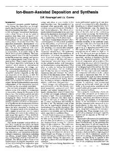
pressure 107 Torr) with a quick sample access system. The ion beam source and plasma source aim at the same point on the sample, see Fig. 1. Variables in the deposition process are the energy and flux of the C' ion beam and the gas species, which is controlled by the power and flux of the plasma source. We fixed the plasma power to -20 Watts and varied the C- ion beam energy because high plasma power (>100 watts) produced no deposition, but etched the substrate. We deposited films on Si, Al, Cu, and zirconia substrates. The Si (100) samples were cleaned to remove the thick intrinsic oxide layer and any residual contaminants before inserting into the deposition chamber. The Si samples were then heated to 850'C to remove any residual oxide layer prior to the deposition and cooled to room temperature. The C beam was formed by the low energy carbon ions sputtered from a graphite target by Cs' ions and accelerating them to a fixed energy. The C' ion current was typically set to -80 PIA and the beam diameter was about 6 2 mm in the 50-150 eV C ion beam energy range. This corresponds to a flux of 4xlO" ions/cm . sec. The flow rate of the N 2 or NH3 gas to the plasma source was controlled by a mass flow controller. In general, about 10 sccm of N 2 or NH 3 flow was used and the deposition pressure was -10"4 Torr. To characterize the deposited films, we employed a standard backscattering Raman spectrometer using the 514.5nm argon ion laser line with 0.75 W incident on the samples. Sample Holder
Sample Insertion
C- Ion Beam Beam Diameter: 05" Beam Energy: 50-150eV
Plasma Beam
RF
j
M.
!
I-
Ion Beam Energy Control Electrode
Csf+
Cs+ Ion Gun Beam Diameter: 0.5" Beam Energy: 3 keV
Graphite
Figure 1.
Schematic diagram of C- ion beam with plasma beam deposition system.
RESULTS AND DISCUSSION
Long range order was not found in our carbon nitride films. TEM and low angle X-ray diffraction were performed and no crystallinity was observed. Nitrogen content in the films, estimated by Auger electron specroscopy depth profiling, was found to be about 50 at. %. Along with nitrogen and carbon, a cesium presence was observed at the level of lower than 1 at.% that could originate from the C' source. Infrared absorption spectra of the carbon nitride films were measured by a Nicolet 800 FTIR system. M. Ricci et al. [7] reviewed possible C:N bondings which are C-N (triple bond) at 2200 cmn1 (nitrile group), C=N (double bond) at 1600 cm"1 (imino group), and C-N (single bond) at 1440 cm" . The structure of P-C 3N4 is believed to be similar to J3-Si 3N 4 with C substituted for Si
as shown in Figure 2a [1]. The unit cell is hexagonal with local order such that C atoms occupy
slightly distorted tetrahedral single bond sites (sp 3 hybridization) while N atoms sit in nearly planar
triply coordinated sites (sp2 hybridization). The correct bonding configuration for the fl-C 3N4
546
phase is the C-N single bond. Fig.2b shows that our films predominantly contain C-N bonds. As shown in Fig. 2b, the ion beam deposited films have no hydr
Data Loading...