Cascode Gallium Nitride HEMTs on Silicon: Structure, Performance, Manufacturing, and Reliability
High-voltage GaN is redefining power conversion, providing cost-competitive and easy-to-embed solutions that reduce costly energy loss by more than 50 %, shrink size and simplify the design and manufacturing of power supplies (for servers, telecom, indust
- PDF / 1,191,239 Bytes
- 18 Pages / 439.37 x 666.14 pts Page_size
- 21 Downloads / 280 Views
Cascode Gallium Nitride HEMTs on Silicon: Structure, Performance, Manufacturing, and Reliability Primit Parikh
10.1
Motivation and Configuration of the Cascode GaN HEMT
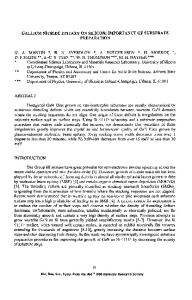
Due to the polarization charges for the AlGaN–GaN heterostructure system [1], GaN HEMTs by nature are depletion mode (d-mode) or normally on devices. While d-mode devices have been successful for RF applications [1], in power switching applications “normally off” devices are mostly preferred for safety and ease of control in the absence of input or control (gate) voltage, when the GaN power device and the associated circuit is off. Unlike the well-established SiO2–Si oxide insulatorsemiconductor system, the lack of a suitable native oxide for the AlGaN–GaN system has hindered the development of enhancement-mode (e-mode) or normally off devices. Although intrinsic e-mode GaN devices have been demonstrated [2, 3], a reliable high-voltage device that performs in a very stable manner in high-voltage applications has been elusive. A cascode GaN HEMT combines a d-mode high-voltage GaN HEMT with a lowvoltage Si MOSFET device to achieve an effective normally off high-voltage device (intrinsically even a Si superjunction transistor is combination of inbuilt low voltage normally off “gating” region and a high voltage normally on “drift/blocking” region). By combining the well-established normally off gating functionality of the Si device with the high-voltage capability of the GaN HEMT, the cascode has enabled a highly reliable, very-high-performance GaN product to the market [4, 5] (Fig. 10.1).
P. Parikh (✉) Transphorm Inc., Goleta, CA 93117, USA e-mail: [email protected] © Springer International Publishing Switzerland 2017 M. Meneghini et al. (eds.), Power GaN Devices, Power Electronics and Power Systems, DOI 10.1007/978-3-319-43199-4_10
237
238
P. Parikh
Fig. 10.1 Schematic of the cascode high-voltage GaN HEMT
10.2
Functionality and Benefits of Cascode GaN HEMT
The operation of the cascode GaN HEMT effectively utilizes the key properties of the Si “driver” FET’s positive threshold voltage and the GaN HEMT’s high off-state blocking. Referring to Fig. 10.2, note that the drain-source voltage of the Si FET is the gate-source voltage of the GaN HEMT. When zero gate voltage is applied to the Si FET, the Si FET turns off first, and its drain to source voltage (VDS1) increases. Since this is the gate-source voltage (VGS2) of the GaN HEMT, it will turn off as soon as this voltage is more negative than its threshold voltage. The HEMT will then block a high off-state voltage (VDS2). When a positive gate voltage is applied to the Si FET (>VTH1), it turns on first, which reduces VDS1 and thus VGS2 to near zero. Hence, the GaN HEMT turns on as its gate-source voltage is now higher than its intrinsic negative threshold voltage. An appropriate Si FET should be chosen whose off-stage voltage is more negative than the GaN HEMT threshold voltage to effec‐ tively turn off the GaN HEMT under all conditions. One of the biggest benefits of the cascode GaN HEMT is the ability to
Data Loading...