Cathodoluminescence microscopy: Optical imaging and spectroscopy with deep-subwavelength resolution
- PDF / 695,133 Bytes
- 7 Pages / 585 x 783 pts Page_size
- 21 Downloads / 377 Views
troduction With the growing importance of nanotechnology, the demand for high-resolution microscopy and characterization techniques has tremendously increased. Conventional optical microscopy is limited in resolution by the diffraction limit for light, making it unsuitable for optical studies at the nanoscale. Near-field optical microscopy,1 in which a nanoscale tip scans over a surface to collect radiation, provides higher spatial resolution but is experimentally complex and often suffers from unavoidable interaction between the tip and the analyzed surface. Other advanced microscopy techniques, such as stimulated emission depletion microscopy,2 photoactivated localization microscopy,3 and stochastic optical reconstruction microscopy,4 show subwavelength resolution but require the use of fluorescent labels. A label-free optical imaging technique with deepsubwavelength resolution, which has recently gained significant
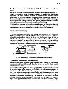
interest, is based on the use of a focused beam of fast electrons as an optical excitation source. As electrons can be focused to nanoscale dimensions, this technique yields deepsubwavelength optical resolution. An electron beam is a very pure optical excitation source. The time-varying evanescent electric field around the electron trajectory can interact with a polarizable medium, resulting in elemental optical materials excitations. These excitations can be probed by studying the energy loss of the electrons (electron energy loss spectroscopy) or by detecting the optical radiation that is subsequently emitted by the material (cathodoluminescence, CL).5 The spatial resolution of excitation is determined by the electron beam spot size, which is on the order of 1 nm, as well as the radial extent of the evanescent electric field about the electron beam, which is on the order of 10 nm, depending on the beam energy. The spectral extent of
Toon Coenen, Center for Nanophotonics, FOM Institute AMOLF, The Netherlands Benjamin J.M. Brenny, Center for Nanophotonics, FOM Institute AMOLF, The Netherlands Ernst Jan Vesseur, Center for Nanophotonics, FOM Institute AMOLF, The Netherlands Albert Polman, Center for Nanophotonics, FOM Institute AMOLF, The Netherlands; [email protected] DOI: 10.1557/mrs.2015.64
© 2015 Materials Research Society
MRS BULLETIN • VOLUME 40 • APRIL 2015 • www.mrs.org/bulletin
359
OPTICAL IMAGING AND SPECTROSCOPY WITH DEEP-SUBWAVELENGTH RESOLUTION
excitation is determined by the interaction time of the electron with the sample, which is typically less than one femtosecond. This is less than one optical cycle of the emitted radiation and corresponds to a broad spectral range, making the moving electron a broadband optical excitation source spanning the ultraviolet/visible/infrared spectral range. Electron beams can also excite materials by impact excitation or through secondary electrons generated inside the material. This incoherent CL emission has been known for decades and is used in the study of optically active semiconductors, quantum dots, lanthanide ions, and radiative point defects in m
Data Loading...