Cavity Nucleation and Evolution in He-Implanted Si and GaAs
- PDF / 2,808,218 Bytes
- 6 Pages / 414.72 x 648 pts Page_size
- 84 Downloads / 388 Views
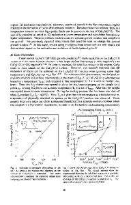
CAVITY FORMATION IN Si Figure la) shows Si implanted with lxl016 He/cm2 at 30 keV and subsequently annealed 1/2 hr. at 700'C. The image was obtained by tilting the layer a few degrees off the [110] zone into a kinematic condition without strong diffraction contrast. Fresnel contrast of the cavities was obtained by underfocussing the microscope by 1.3 tim. The cavities are in isolated clusters near the He projected range, Rp = 300 nm, and their lateral density is not uniform. Often there is a larger central cavity (-50 nm across) with smaller cavities (5-10 nm) around it, like one of the clusters in Fig. la). The •resence of cavities at this fluence agrees with their detection by positrons for 8x10¹⁵ He/cm [10]. Residual diffraction contrast around the clusters in Fig. la) reflects the presence of strain fields from lattice defects localized on the clusters. Imaging with (111) and (220) two-beam conditions (not shown) indicates the presence of {11 } planar defects near the clusters as well as defects parallel to the surface and passing through the cluster centers. Figure lb) is from Si implanted with 2x10 He/cm2 at 30 keV after 1/2 hr. at 700TC, and shows a layer of cavities 65 nm wide and located at Rp, with an approximately uniform lateral density. We label such layers "continuous". Some larger cavities (20-40 nm) are seen in the layer; the clusters in Fig. la) suggest that the larger cavities may have formed first. Smaller cavities (5-10 nm) lie on "strings" connecting the larger ones, as if the clusters in Fig. la) increased in width until they connected with each other. These strings suggest that their cavities lie on dislocations. The inset in Fig. lb) was taken with (111) two-beam diffracting conditions and shows strain fields around the entire layer, as expected for connecting dislocations. Figure Ic) shows a TRIM90 [11] Monte Carlo simulation of the He profile for 2x10 16 He/cm 2 at 30 keV, after scaling the range slightly to fit the observed 300 nm. The implanted He concentration is thought to be the critical parameter determining whether numerous stable cavities form during the 1/2 hr. anneal at 7001C. The peak concentration required for a layer with an essentially uniform lateral density of cavities lies between those of the two fluences of Figs. Ia) and I b), and is close to the latter. Using the 65 nm width with the He profile gives a threshold of 1.6 at.% He, as shown by the dashed lines in Fig. lc). With 2x10 He/cm , the cavity surface area is sufficient to getter 8xl014 Cu/cm2 [12], whereas the isolated clusters for lxlO16 He/cm2 do not getter a significant amount of Cu. Thus 2x10¹⁶ He/cm2 is also a practical threshold fluence for gettering metal impurities. We also attempted to increase the cavity area and number density while maintaining a narrow layer by implanting an additional 5x10⁶ He/cm2 into the structure of Fig. Ib). To allow the additional He to collect at the existing layer, the second implantation was done at 500'C. The size and perhaps the density of cavities in the layer at Rp = 300 n
Data Loading...