CdS and CdTe Large Area Thin Films Processed by Radio-Frequency Planar-Magnetron Sputtering
- PDF / 85,108 Bytes
- 5 Pages / 595 x 842 pts (A4) Page_size
- 64 Downloads / 403 Views
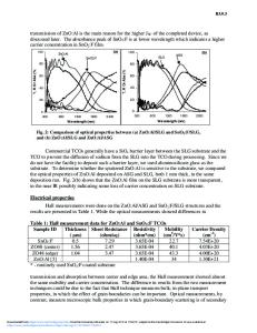
CdS and CdTe Large Area Thin Films Processed by Radio-Frequency PlanarMagnetron Sputtering* H. Hernández-Contreras, G. Contreras-Puente, J. Aguilar-Hernández, A. MoralesAcevedo(1), J. Vidal-Larramendi(2) and O. Vigil-Galan(2) Escuela Superior de Física y Matemáticas del Instituto Politécnico Nacional, Edificio 9, UPALM 07738 Mexico, D. F. (1) Permanent address: Departamento de Ingeniería Eléctrica, CINVESTAV del IPN, Mexico, D. F. (2) Permanent address: Facultad de Física-IMRE, Universidad de la Habana, 10400, Cd. Habana Cuba. ABSTRACT The processing of large area thin films solar cells represents a challenge, mainly due to the need for optimal setting of the critical growth parameters for scaling-up of the processes that guarantee homogeneous properties in the sub-minimodule architecture. We have been working with a Radio-Frequency Planar Magnetron Sputtering (RF-PMS) system, processing 450 cm2 areas of CdS and CdTe thin films grown on soda lime glasses and conducting glasses (SnO2:F-7Ω/ ) for CdS, using for it a 6’’ balanced gun. The films have been processed with substrate temperatures (Ts) of 250°C, Ar chamber-pressure of 20 mTorr, and radio frequency power of 300 watts. The films were characterized by morphological, optical and electrical techniques, presenting in this work the corresponding measurements. Our results show that the better polycrystalline perfection, adherence and pinhole free films are obtained at substrate temperatures of 250°C. INTRODUCTION The manufacturing of large area photovoltaic devices implies the optimization of critical growth parameters in a given processing system. Sometimes, this knowledge is gained during the processing of prototype solar cells at a smaller scale and with less complex growth systems. The complications arise whenever the process is projected to a large scale system. The sputtering process and in particular the one controlled by the use of magnetic fields, namely the RF-PMS is a promising scaling-up processing technique for II-VI solar cells. In a previous work we have studied the optimal setting of the different critical growth parameters on the properties of large area CdS and CdTe thin films, with optimal Ts at 250°C [1]. We present in this work the results of large area RF-PMS CdS and CdTe thin films grown on soda lime glass and on conducting glass for CdS. EXPERIMENTAL DETAILS Details of the depositing procedure of CdS and CdTe were previously reported [1]. We describe here briefly the system. The basic system is conformed by two opposite guns of 6’’. The movable substrate is fixed on a heater, through an automatic carrier and there are four optical ports for controlling the thickness of the films. An automatic carrier makes it possible to grow uniform films along a 1 feet (30 cm) long surface. The substrate can be rotated in order to get, first a deposition of a CdS film, and without breaking the vacuum, to deposit a second film of CdTe. H8.5.1
With this system we have grown films of CdS and CdTe varying growth parameters such as the substrate temperature (T
Data Loading...