Characteristics of deep traps in freestanding GaN
- PDF / 136,132 Bytes
- 6 Pages / 612 x 792 pts (letter) Page_size
- 111 Downloads / 388 Views
Characteristics of deep traps in freestanding GaN Z-Q. Fang1, D.C. Look1, P. Visconti2, C. Lu2, D. Wang2, H. Morkoç2, S.S. Park3, and K.Y. Lee3 Semiconductor Research Center, Wright State University, Dayton, OH 45435 2 Electrical Engineering and Physics Department, Virginia Commonwealth University, P. O. Box 843072, Richmond, VA 23284-3072 3 Samsung Advanced Institute of Technology, P. O. Box 111, Suwon, Korea 440-600 1
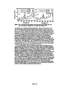
ABSTRACT Deep traps in a 300-µm-thick freestanding GaN sample were characterized by deep level transient spectroscopy (DLTS), using Schottky barrier diodes (SBDs) fabricated on the Ga polarity surface. Most of the SBDs show nearly ideal current-voltage characteristics, with both forward and reverse currents controlled by the thermionic emission mechanism. Five common traps, which include A1 (1.0 eV), A (0.66 eV), B (0.59 eV), C (0.35 eV), and D (0.25 eV), can be consistently observed in all SBDs. Two of them, A1 and C, are related to surface damage. Surprisingly, some new traps can be found in the DLTS spectra of some SBDs if higher reverse biases are used in the measurements. However, they cannot be fitted by DLTS simulations, and are likely associated with parasitic capacitance somewhere in the cryostat. INTRODUCTION Hydride vapor phase epitaxy (HVPE) is a promising technique for growing thick GaN layers because of the high growth rates attainable [1]. A process to separate HVPE GaN layers from Al2O3 substrates has been developed [2] and it has been proposed that the separated templates (so-called freestanding GaN) can themselves be used as substrates for further GaN growth. Recently, freestanding GaN has demonstrated the excellent quality of such material in terms of electrical, optical, and structural properties [3-8]. This material has the highest GaN mobility ever measured (1245 cm2/V-s at 300 K), and the lowest donor and acceptor concentrations, about 6.7 x 10¹⁵ and 1.7 x 1015 cm-3, respectively [5]. In addition to very sharp near-band-edge emissions, photoluminescence studies reveal the presence of both yellow and green luminescence, the observation of which depends on excitation energies and intensities [7]. The density of dislocations near the Ga face, revealed by cross-sectional TEM, can be as low as 5 x 106 cm-2 [8]. However, some inhomogeneities of near-band-edge and yellow emissions in the cathodoluminescence spectra have been reported and correlated with the crystalline structure [9]. Deep traps, near both Ga and N faces, in a freestanding GaN sample (#89) have been recently characterized by deep level transient spectroscopy (DLTS) [10], and a new trap B′ with an anomalous capture behavior was reported, in addition to five common DLTS traps, which had been observed previously in various epitaxial GaN layers. In this paper, we report on currentvoltage (I-V) and trap characteristics for twelve Schottky barrier diodes fabricated on a different piece of freestanding GaN sample (#135). The observed deep traps can be classified into two groups. The first group covers common deep traps, i.e.
Data Loading...


