Characterization of boron nitride thin films prepared from a polymer precursor
- PDF / 311,586 Bytes
- 8 Pages / 612 x 792 pts (letter) Page_size
- 106 Downloads / 311 Views
MATERIALS RESEARCH
Welcome
Comments
Help
Characterization of boron nitride thin films prepared from a polymer precursor V. Z-H. Chan Laboratory for Research on the Structure of Matter, and Department of Materials Science and Engineering, University of Pennsylvania, Philadelphia, Pennsylvania 19104
J. B. Rothman Laboratory for Research on the Structure of Matter, University of Pennsylvania, Philadelphia, Pennsylvania 19104
P. Palladino Laboratory for Research on the Structure of Matter, and Department of Materials Science and Engineering, University of Pennsylvania, Philadelphia, Pennsylvania 19104
L. G. Sneddon Laboratory for Research on the Structure of Matter, and Department of Chemistry, University of Pennsylvania, Philadelphia, Pennsylvania 19104
R. J. Composto Laboratory for Research on the Structure of Matter, and Department of Materials Science and Engineering, University of Pennsylvania, Philadelphia, Pennsylvania 19104 (Received 10 July 1995; accepted 10 October 1995)
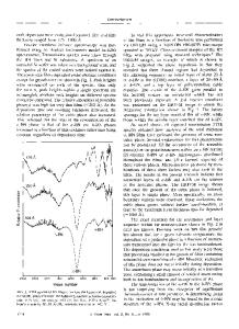
Excellent quality boron nitride (BN) thin films on silicon have been produced by a simple procedure involving spincoating solutions of the “single-source” polymericprecursor polyborazylene, (B3 N3 H,4 dx , on a silicon substrate, followed by pyrolysis at 900 ±C. Rutherford backscattering spectrometry (RBS) indicates that the ByN ratios are 1.37 and 1.09 for conversions carried out in a vacuum oven at 900 and 1250 ±C, respectively. Forward recoil spectrometry (FRES) showed that the atomic percent of residual hydrogen is 10 and 9%, respectively. Plain-view and cross-sectional scanning electron microscopy (SEM) studies showed that the samples annealed at 900 ±C were clean and uniform in thickness. A thickness of 800 3 1015 atomsycm2 was determined by ion scattering. Films annealed to 1250 ±C likewise showed a continuous unbroken boron nitride layer, but also exhibited morphological features resulting from reactions of the underlying silicon oxide-silicon interface in the substrate. Auger electron spectroscopy and atomic force microscopy showed that the BN coating produced at this higher temperature remained unbroken but had a surface area of ,15% covered by dimples 2–7 nm in depth. Compared to typical films made by chemical vapor deposition, BN films produced from this “single-source” method have lower hydrogen and carbon concentrations.
I. INTRODUCTION
Boron nitride (BN) thin films have a wide range of attractive properties including high temperature stability, a low dielectric constant, strength, large thermal conductivity, hardness, and corrosion resistance, leading to a number of potential applications as structural and electronic materials.1 Vapor deposition techniques have received a great deal of attention for preparing BN films.1 For electronic applications requiring electrically insulating layers on semiconductors, chemical vapor deposition (CVD) has proven to be a very useful preparation technique.2–9 In this method a single chemical precursor or mixture is decomposed at or above a substrate surface to form the desired BN fi
Data Loading...