Phase evolution in boron nitride thin films
- PDF / 611,980 Bytes
- 4 Pages / 576 x 791 pts Page_size
- 40 Downloads / 368 Views
K. L. More High Temperature Materials Laboratory, Mailstop 6064, Oak Ridge National Laboratory, Oak Ridge, Tennessee 37831-6064 (Received 13 November 1992; accepted 19 January 1993)
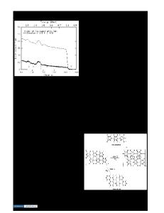
Boron nitride (BN) thin films were deposited on monocrystalline Si(100) wafers using electron beam evaporation of boron with simultaneous bombardment by nitrogen and argon ions. The effect of film thickness on the resultant BN phase was investigated using Fourier transform infrared (FTIR) spectroscopy and high resolution transmission electron microscopy (HRTEM). These techniques revealed the consecutive deposition of an initial 20 A thick layer of amorphous BN, 20-50 A of hexagonal BN having a layered structure, and a final layer of the polycrystalline cubic phase. The growth sequence of the layers is believed to result primarily from increasing biaxial compressive stresses. Favorable surface and interface energy and crystallographic relationships may also assist in the nucleation of the cubic and the hexagonal phases, respectively. The presence of the amorphous and hexagonal regions explains why there have been no reports of the growth of 100% cubic boron nitride on Si.
Boron nitride is similar to carbon in having three crystalline structures1: a layered hexagonal structure (/i-BN) corresponding to graphite, the cubic structure (c-BN) analogous to diamond, and a rare hexagonal wurtzite structure (w-BN) corresponding to Lonsdaleite. The last two phases are metastable under normal environmental conditions. An amorphous phase (a-BN) is also common in films and coatings. The extreme mechanical and thermal properties of c-BN make it useful or potentially useful for wearresistant tools for the machining of steels, for corrosionresistant and electrically insulating parts, and for heat sinks for electronic devices. It has also recently been shown that bulk single crystals of this wide bandgap (Eg = 6.4 eV) semiconductor can be doped with both n- and p-type impurities and that light emitting p-n junctions can be produced.2 This phase, combined with other BN phases, has also been achieved in thin film form via physical vapor deposition3"5 and chemical vapor deposition5 methods. Most researchers growing BN films use FTIR spectroscopy for phase identification. The cubic phase of BN has a distinct absorption peak at about 1080 cm"1. The hexagonal [graphitic or turbostratic (randomly rotated arrangement of hexagonal layers)] and amorphous phases have primary and secondary absorption peaks at 1370 and 780 cm"1, respectively. Thus, these noncubic phases cannot be distinguished using FTIR. A J. Mater. Res., Vol. 8, No. 6, Jun 1993 http://journals.cambridge.org
Downloaded: 01 Feb 2015
commonly reported feature of these spectra obtained from analyses through the total thickness of the films, wherein the presence of c-BN is apparent, is the indication of various amounts of the hexagonal and/or amorphous phases (see, e.g., Refs. 4 and 5). The FTIR spectra of the films obtained in the present research showed similar results. However, the unusual evoluti
Data Loading...


