Characterization of Dislocations and Interfaces in Semiconductors by High Resolution Electron Microscopy
- PDF / 1,319,341 Bytes
- 6 Pages / 417.6 x 639 pts Page_size
- 85 Downloads / 372 Views
Inc.
279
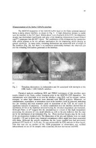
CHARACTERIZATION OF DISLOCATIONS AND INTERFACES RESOLUTION ELECTRON MICROSCOPY
J.C.H. SPENCE and A. OLSEN Dept. of Physics, Arizona State University,
IN SEMICONDUCTORS
Tempe,
AZ
BY HIGH
85281
ABSTRACT It is not presently possible to resolve the individual atoms in any semiconductor by high resolution electron microscopy (HREM). However symmetry arguments may be used to allow near-atomic resolution lattice images to be interpreted in rare favorable cases. This method is applied to the problem of distinguishing shuffle and glide set partial dislocations in silicon. It is also proposed that two dimensional characteristic loss energy selected diffraction patterns be used to reveal the local symmetry about selected substitutional species implanted in semiconductor lattices.
INTRODUCTION While structure imaging by high resolution transmission electron microscopy has given crystal chemists new insight into many defect structures and phase transformation mechanisms in recent years, there have been few, if any, really useful results from this technique in the field of semiconductor physics. This is chiefly because it is not presently possible to obtain a structure image at atomic resolution of any common semiconductor. Here a structure image is defined as a lattice image which faithfully reveals a crystal's structure to some limited resolution and which was recorded under instrumental conditions which are independant of the structure. "Tuning" the electron microscope to the structure results, in general, in an uninterpretable lattice image in small unit cell crystals. Thus the major limitations of the high resolution TEM technique for semiconductors are (i) the need to extract structural information from images beyond the current 2.7A Scherzer point resolution limit, (ii) the insensitivity of these images to atomic displacements in the electron beam or projection direction, (iii) the difficulty of extracting chemical or atomic number information from the images. Approaches to each of these problems are discussed in the following. THREE-DIMENSIONAL INFORMATION Fault vector components in the beam direction may, in favorable cases, be found from convergent beam patterns recorded from the same area from which a lattice image has been obtained. The instrumental compatability of the CBED and structure imaging techniques has been described elsewhere [1]. Frequently, the destruction by strain of the three dimensional interference condition needed to produce fine HOLZ and Kikuchi lines in CBED patterns may be used to obtain several "g.b = 0" conditions from a single CBED pattern, thus allowing an out-of-ZOLZ g to be found from a single microdiffraction pattern [2]. This three-dimensional information is usually impossible to extract from lattice images. Further, if HOLZ lines are used, this technique does not require the sample to be tilted from the zone axis lattice imaging orientation - an important consideration in view of the very limited tilt available (100) on modern HREM machines. There is thus an urgent nee
Data Loading...