Characterization of Electroplated Copper Films with Laser-Generated Surface Acoustic Waves
- PDF / 867,953 Bytes
- 6 Pages / 612 x 792 pts (letter) Page_size
- 5 Downloads / 217 Views
E3.21.1
Characterization of Electroplated Copper Films with Laser-Generated Surface Acoustic Waves A.A. Maznev1, M. Gostein1, and S.H. Brongersma2, 1 Philips Advanced Metrology Systems, 12 Michigan Dr., Natick MA 01760, U.S.A. 2 IMEC, Kapeldreef 75, B-3001, Leuven, Belgium ABSTRACT Elastic properties of electroplated copper films fabricated under different plating and annealing conditions have been characterized with laser-generated surface acoustic waves. For acoustic wavelengths longer than the characteristic copper grain size, the effective elastic modulus of copper was found to be unaffected by variations of the plating current as well as by the grain size variation due to different annealing temperatures. Consequently, copper thickness measurements with surface acoustic waves have been found to be more stable with respect to process variations than electrical sheet resistance measurements. For short acoustic wavelengths ( ~ 2 µm), grain growth results in a significant increase of acoustic attenuation and a shift in the measured velocity. This finding opens an opportunity for copper structure monitoring by surface wave-based optoacoustic metrology.
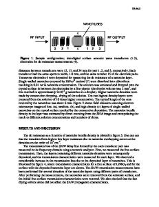
INTRODUCTION Electro-chemical deposition (ECD) of copper followed by chemical-mechanical polishing (CMP) is the main method of fabrication of metal interconnects for state-of-the-art integrated circuits. It is known that copper microstructure is strongly affected by the parameters of the plating process and subsequent annealing [1,2]. In particular, a dramatic grain growth is known to follow the plating even at room temperature. A high-temperature anneal facilitates further grain growth, with final grain size typically on the order of a few µm for a 1 µm-thick film, which is tens of times larger than the initial as-plated grain size. The purpose of the present study is to find out whether the variations in the process conditions determining the microstructure also affect the elastic properties of Cu films. We fabricated a matrix of samples representing a variety of plating and annealing conditions and characterized them with surface acoustic waves (SAWs), an approach widely used for mechanical characterization of thin films [3]. The present study was also partially motivated by previous observations of a measurable change in the SAW velocity during room-temperature annealing of electroplated Cu films [3]. SAW measurements were done using a Philips AMS SurfaceWave™ thin film metrology system which uses lasers for both excitation and detection of SAWs. The system is designed for film thickness measurements but is also capable of elastic properties characterization [4].
EXPERIMENT Four 200 mm Si (100) wafers coated with 50 nm CVD-deposited SiN and 500 nm SiO2 were used. First, a 30 nm TaN/Ta diffusion barrier followed by a 100 nm seed copper layer were
Downloaded from https://www.cambridge.org/core. University of Texas Libraries, on 06 Jan 2020 at 12:38:55, subject to the Cambridge Core terms of use, available at https://www.cambridge.org/core/terms. https://doi.org/
Data Loading...