Mechanisms for Microstructure Evolution in Electroplated Copper Thin Films
- PDF / 958,001 Bytes
- 6 Pages / 417.6 x 639 pts Page_size
- 118 Downloads / 461 Views
IBM T.J. Watson Research Center, Yorktown Heights, NY 10598 ABSTRACT
We present a model which accounts for the dramatic evolution in the microstructure of electroplated copper thin films near room temperature. Microstructure evolution occurs during a transient period of hours following deposition, and includes an increase in grain size, changes in preferred crystallographic texture, and decreases in resistivity, hardness and compressive stress. As the grain size increases from the as-deposited value of 0.05-0.1 gm up to several im, the decreasing grain boundary contribution to electron scattering lowers the resistivity by tens of percent to near-bulk values. Concurrently, as the volume of grain boundaries decreases, the stress is shown to change in the tensile direction by tens of MPa. The as-deposited grain size is also shown to be consistent with grain boundary pinning. INTRODUCTION Electroplating is being used to fill small high-aspect ratio features with copper
interconnections for silicon chip technology (1). Several groups (2-7) have reported that the resistivity of as-deposited electroplated copper exceeds the bulk value of 1.7 JLQ--cm by 10-30%, but after a transient period of hours at room temperature, the resistivity decreases to near-bulk values. Concurrently, the grain size increases by about an order of magnitude. We present a consistent set of mechanisms which accounts for the major property changes during this transient period, driven by the reduction of grain boundary energy stored in the as-deposited
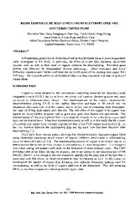
microstructure. In one study of room temperature transients in electroplated copper thin films by Cabral et al. (2), the copper films were typically 1gtm thick, electrodeposited onto sputtered
copper underlayers. Measurements of resistivity and stress vs. time at room temperature (21°C) from this work are reproduced in Fig. 1, showing a 20% decrease in the resistivity over a period of 9 hours, coupled with a stress change from -45 MPa (compressive) to near zero. Focused ion beam (FIB) measurements on the same samples (2,8) show that the grain size increases from typically 0.05-0.1 gm up to several gm during this transient period. Large grains are found to nucleate and grow within a background of small grains, indicating a process of abnormal grain growth (9). We first discuss the resistivity transient, then the stress change and pinning mechanisms. EFFECT OF GRAIN SIZE ON RESISTIVITY Several mechanisms are capable of increasing the resistivity of copper above its room temperature value of 1.7 ji.Q-cm (10). They all decrease the electron mean free path from the
387
Mat. Res. Soc. Symp. Proc. Vol. 564 01999 Materials Research Society
(a)
.•
1
2d.
E' 23
. 20% decrease
22
",20
2
21-
intrinsic room temperature value of 39 nm for single crystal copper (11). The additional processes include scattering from defects including vacancies, impurity atoms, dislocations, grain boundaries and second phase particles, plus non-specular scattering from the top
_____,.__1_____
surface, bottom interfac
Data Loading...