Characterization of GaAs Surfaces Subjected to A Cl 2 /Ar High Density Plasma Etching Process
- PDF / 336,983 Bytes
- 5 Pages / 414.72 x 648 pts Page_size
- 38 Downloads / 359 Views
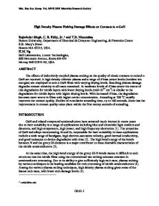
0.8 mm dia.
Stainless Steel fr~ont plate '--. I
GaAs
"•
BN Ceramic Heater
Copper 0 0 Copper cooling lines
0.)
0
Figure 1. The front cap is designed to emulate a traditional etching stage with full temperature control (both heating and cooling capabilities). When examining the surface chemistry, process conditions were varied as: total pressure = 0.5-5 mTorr, coupled microwave power = 200-500 W, and rfinduced dc bias = 0-400 V. The mass spectrometer is calibrated using both perfluorotributlyamine (which contains major peaks at 69, 131 and 219) and etch product samples of AsC13 and GaCI3. These efforts resulted in excellent calibration
0
-5.600"
over the range of etch product masses (100-
.0
Figure 1. Schematic diagram of mass spectrometer front cap/sampling aperture.
190 amu). A critical process parameter in investigating surface chemistry issues in a
high density plasma etching process is the substrate temperature. Accurate measurement of this parameter is important to assigning thermal and ion-assisted chemical etch processes occurring at the surface. As anisotropic pattern transfer is desired, ion-assisted chemistry is preferred with minimal variation in thermal chemistry. In this work, diffuse reflectance spectroscopy [2] is used to determine the temperature of the substrate itself. In this technique, the shift in the position of the absorption edge of the semiconductor is measured. This shift corresponds to the change in the band gap which is a well-defined function of temperature[3]. Application of this technique to the highly emissive environment of a plasma processing reactor requires substantial efforts to achieve good signal-to-noise ratios. A schematic of our experimental configuration is shown in Figure 2. In this application, both lock-in amplification and post sample wavelength selection are employed to improve signal to noise. The
technique gives 6A/°C resolution and signal-to-noise ratios of 10:1. Surface damage is evaluated by measuring (with photoreflectance) the position of the surface Fermi level before and after the sample is subjected to plasma etching. The photoreflectance technique is described in full detail elsewhere [4].
In short, the built-in electric
field (E_Es)at the surface is Si p/n diode
measured reflectance above
Monochiromator
by the change in (at wavelengths just
the
band
gap)
of
the
semiconductor surface as hv>Eg radiation is applied to that surface. The built-in electric field is defined as:
S Chopper
as
,1
(1)
Ei d 45WatQuart
•where
EF is the Fermi level at the
45 Watt Quartz
surface, Ec/•
Halogen Lamp
band or valence band energy levels
is the conduction
for UN or UP samples, respectively, and d is the thickness of the undoped layer. The etch
Mass Spectrometer Figure 2. Schematic diagram of diffuse reflectance spectroscopy apparatus used to monitor substrate temperature
34
process can effect both d and EF so it is necessary to measure d
using independent step height measurements (performed here using a Tencor Alphastep 250). RESULTS
Data Loading...