Characterization of GaS-Passivated Quantum-Well Laser Diodes
- PDF / 416,239 Bytes
- 6 Pages / 420.48 x 639 pts Page_size
- 21 Downloads / 332 Views
Mat. Res. Soc. Symp. Proc. Vol. 573 © 1999 Materials Research Society
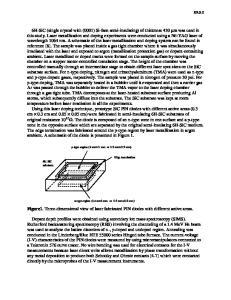
significant increase in the maximum achieved output power without COD.15 However, the significant disadvantage of this process is that the results are only temporary. In addressing the transient nature of sulfur-containing solution treatments, a more stable passivation for GaAs surfaces has been demonstrated using metalorganic chemical vapor deposition (MOCVD) grown gallium sulfide films.' 0 These films demonstrated a high degree of surface passivation; so much as to unpin the Fermi level," and furthermore, maintain their stability for an extended period of time. Although many GaAs surface passivation processes have been studied, the effects of these films are more often tested on metal-insulator-semiconductor (MIS) devices and less often on laser diodes. In this presentation, we investigate the effects of GaS passivation on ridge waveguide AlGaAs/GaAs quantum-well laser diodes. Unpassivated laser diodes are compared with those passivated using different surface preparations. The passivation of the laser diode facets using an MOCVD gallium sulfide film after removing the native oxide gives results consistent with a substantial reduction in the surface states and, therefore, a measurable increase in peak output power before COD. EXPERIMENT The laser diodes were fabricated concurrently from the same Center for High Technology Material (CHTM)-grown AlGaAs/GaAs multiquantum-well structure wafer, which emits light at 825 nm. All samples were processed using a 9-micron ridge waveguide process. The ridges were etched in the starting material then the entire surface was covered with a plasma-enhanced chemical vapor deposition (PECVD) silicon nitride film to provide electrical isolation. P-side openings were etched through the silicon nitride on the tops of the ridges. This was followed by e-beam evaporation of two levels of Ti/Pt/Au metallization on the front side of the wafer to form the p-side contact of the devices. The backside of the wafer was then thinned and metallized with Ni/Ge/Au/Ag/Au to form the n-side contact of the device. The completed wafer of laser diodes was cleaved at 500-ptm intervals to yield bars of twenty electrically isolated devices each. For the purpose of this study, three separate facet coatings were investigated. These were designated as '374', 'TQI' or 'TQ5' (see Table I for details) and present a matrix of facet preparations that allow the relative contributions of electronic versus physical passivation to be established for the applied GaS coatings. After cleaving, the 374 control sample and the TQ1 samples were separated and the TQ5 sample were dipped in ammonium sulfide to remove the native oxide. It must be noted that the ammonium sulfide in this case is not thought to contribute to the actual passivation but merely provides a method of surface cleaning. This is based upon an earlier comparison of GaAs surface photoluminescence for surfaces prepared by either ammonium sulfide immersion, under an inert atmosphere in a g
Data Loading...