Characterization of photovoltaics with In 2 S 3 nanoflakes/ p -Si heterojunction
- PDF / 847,061 Bytes
- 7 Pages / 595.28 x 793.7 pts Page_size
- 29 Downloads / 296 Views
NANO EXPRESS
Open Access
Characterization of photovoltaics with In2S3 nanoflakes/p-Si heterojunction Yu-Jen Hsiao1*, Chung-Hsin Lu2, Liang-Wen Ji3*, Teen-Hang Meen4, Yan-Lung Chen3 and Hsiao-Ping Chi5
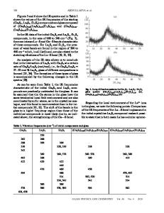
Abstract We demonstrate that heterojunction photovoltaics based on hydrothermal-grown In2S3 on p-Si were fabricated and characterized in the paper. An n-type In2S3 nanoflake-based film with unique ‘cross-linked network’ structure was grown on the prepared p-type silicon substrate. It was found that the bandgap energy of such In2S3 film is 2.5 eV by optical absorption spectra. This unique nanostructure significantly enhances the surface area of the In2S3 films, leading to obtain lower reflectance spectra as the thickness of In2S3 film was increased. Additionally, such a nanostructure resulted in a closer spacing between the cross-linked In2S3 nanostructures and formed more direct conduction paths for electron transportation. Thus, the short-circuit current density (Jsc) was effectively improved by using a suitable thickness of In2S3. The power conversion efficiency (PCE, η) of the AZO/In2S3/textured p-Si heterojunction solar cell with 100-nm-thick In2S3 film was 2.39%. Keywords: Heterojunction; Nanoflake; In2S3
Background Indium sulfide (In2S3) is one of the important semiconductor materials with direct bandgap and attracts intense interest due to its high photosensitivity, photoconductivity, and photocatalyst characteristics at ambient conditions [1-3]. In In2S3, there are three polymorphic forms: defect cubic structure α-In2S3, defect spinel structure β-In2S3, and higher-temperature-layered structure γ-In2S3 [4]. Among them, β-In2S3 is an n-type semiconductor with superior photoelectric conversion function that can be employed in near-infrared to ultraviolet regions of solar energy absorption [5]. Hence, we may expect that β-In2S3 will act as a good absorber in heterojunction thin film solar cells [6]. On the other hand, In2S3 is a nontoxic semiconductor material which also offers potential advantage in process without Cd and Pb. A cell with ITO/ PEDOT:PSS/In2S3:P3HT/Al structure has been fabricated by Jia et al. [7], which showed the short-circuit current density (Jsc) of 0.68 mA cm−2 and a power conversion efficiency of 0.04%.
* Correspondence: [email protected]; [email protected] 1 National Nano Device Laboratories, No. 27, Nanke 3rd Rd., Xinshi District, Tainan 74147, Taiwan 3 Institute of Electro-Optical and Materials Science, National Formosa University, Wénhuà Rd., Huwei, Yunlin 632, Taiwan Full list of author information is available at the end of the article
In recent years, In2S3 thin films have been grown by a variety of deposition techniques such as chemical bath deposition (CBD) [8], thermal evaporation [9], solvothermal synthesis [10], and atomic layer chemical vapor deposition (ALCVD) [11]. Among them, chemical bath deposition is a desirable method because of its low cost, arbitrary substrate shapes, simplicity, and can be easily prepared in large areas. There have been many reports for the
Data Loading...